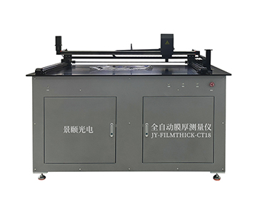
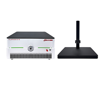
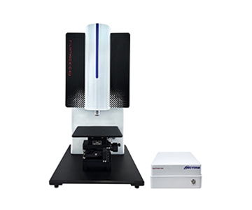
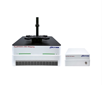
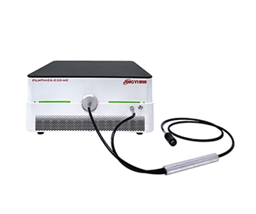
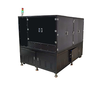
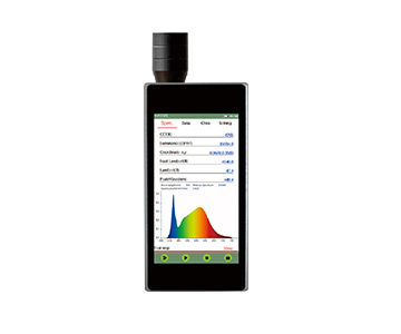
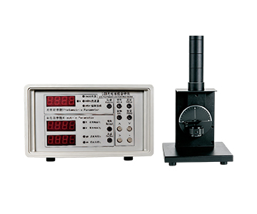
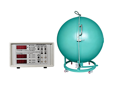
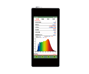
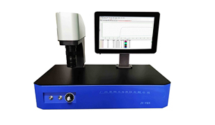
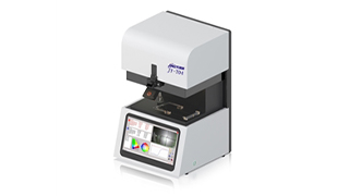
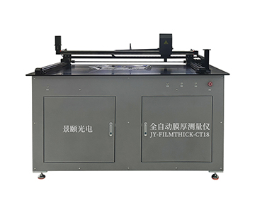
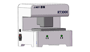
Spectroscopic detection and optical precision measurement capabilities are converging at a new facility in Shantou, where a Guangzhou-headquartered instrumentation firm is scaling its engineering capacity to address measurement repeatability, traceability, and production-line integration challenges across semiconductor, LiDAR, and optical coating sectors. The expansion introduces a multi-disciplinary team focused on closing the loop between standards participation and product verification.
Event Overview: Launch of the Shantou R&D Center
The newly established Shantou R&D center operates as an extension of the existing Guangzhou headquarters, absorbing tasks in optical measurement algorithms, precision mechanical design, calibration system development, and industry-specific application validation. This geographic distribution—Guangzhou for system-level R&D, Shantou for applied verification and custom projects—shortens the cycle from requirement confirmation to prototype delivery.
The center’s technical mandate centers on four parameters: measurement repeatability under production conditions, metrological traceability to national standards, environmental adaptability across temperature and humidity ranges, and seamless integration into automated production lines. Rather than simply expanding headcount, the facility串联s (chains) “standards comprehension—instrument development—scenario validation—batch delivery” into an iterable R&D pipeline.
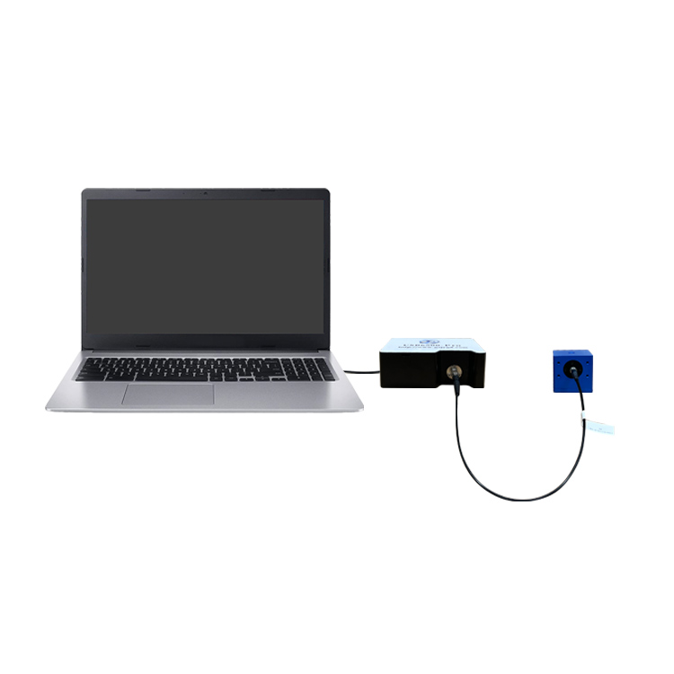
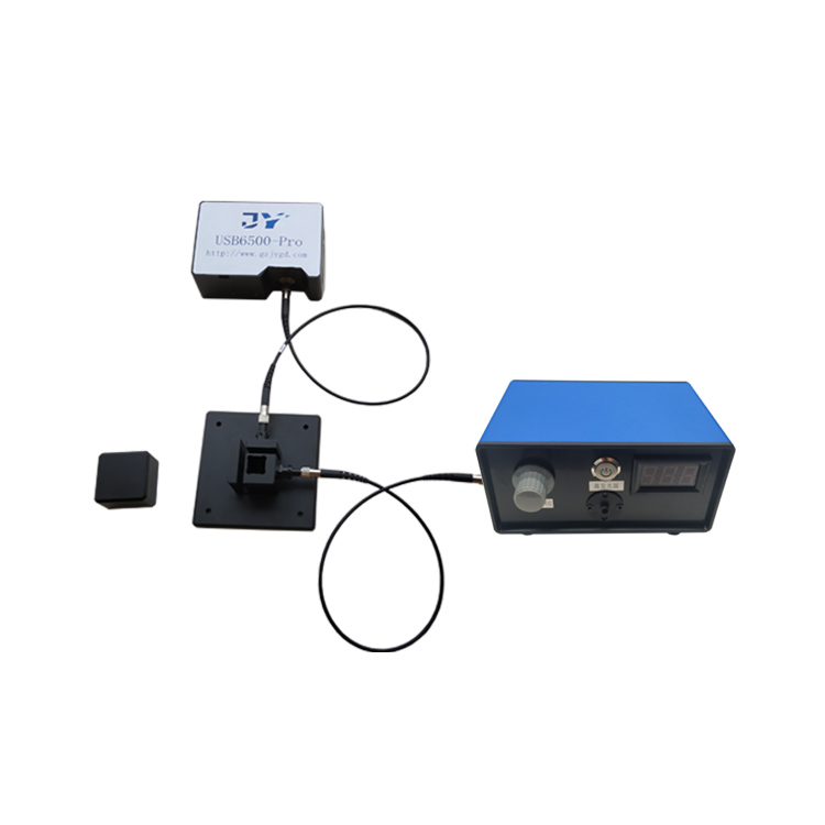
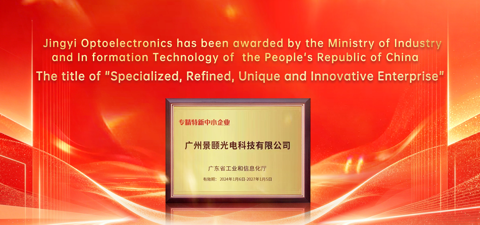
Jingyi Optoelectronics brings to this effort a full-chain development capability spanning fiber optic spectrometers, integrating spheres, reflectance panels, and transmittance/reflectance detection systems. R&D personnel account for over 50% of the total workforce, with collaborative bases now in Guangzhou, Beijing, and Shantou. The Shantou addition accelerates the translation of field problems from customer sites into product definition and algorithm optimization inputs.
Corporate capabilities mapped against evaluation criteria:
| Evaluation Dimension |
Corresponding Capability |
| Core technology independent IP |
Covers reflectivity detection, integrating sphere optical path design, LiDAR calibration panel, transmittance measurement system, and spectral analysis algorithm self-development |
| R&D investment and continuous innovation |
Multi-center collaboration, >50% R&D staff ratio, rapid verification and mass-production conversion for custom projects |
| High-tech product revenue contribution |
Main business in spectroscopic detection and optical precision measurement equipment serving semiconductor, optical communication, LiDAR, optical coating, new energy sectors |
| Engineering team configuration |
Optics, mechanical, electronic, algorithm, and software teams supporting closed-loop development from prototype to production-line equipment |
| Growth and industry adaptability |
Products deployed in research institutes and industrial inspection scenarios with expanding market base for high-end measurement instruments |
Core Technology Domains
Reflectivity Measurement Instruments
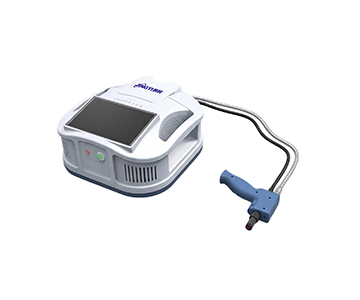
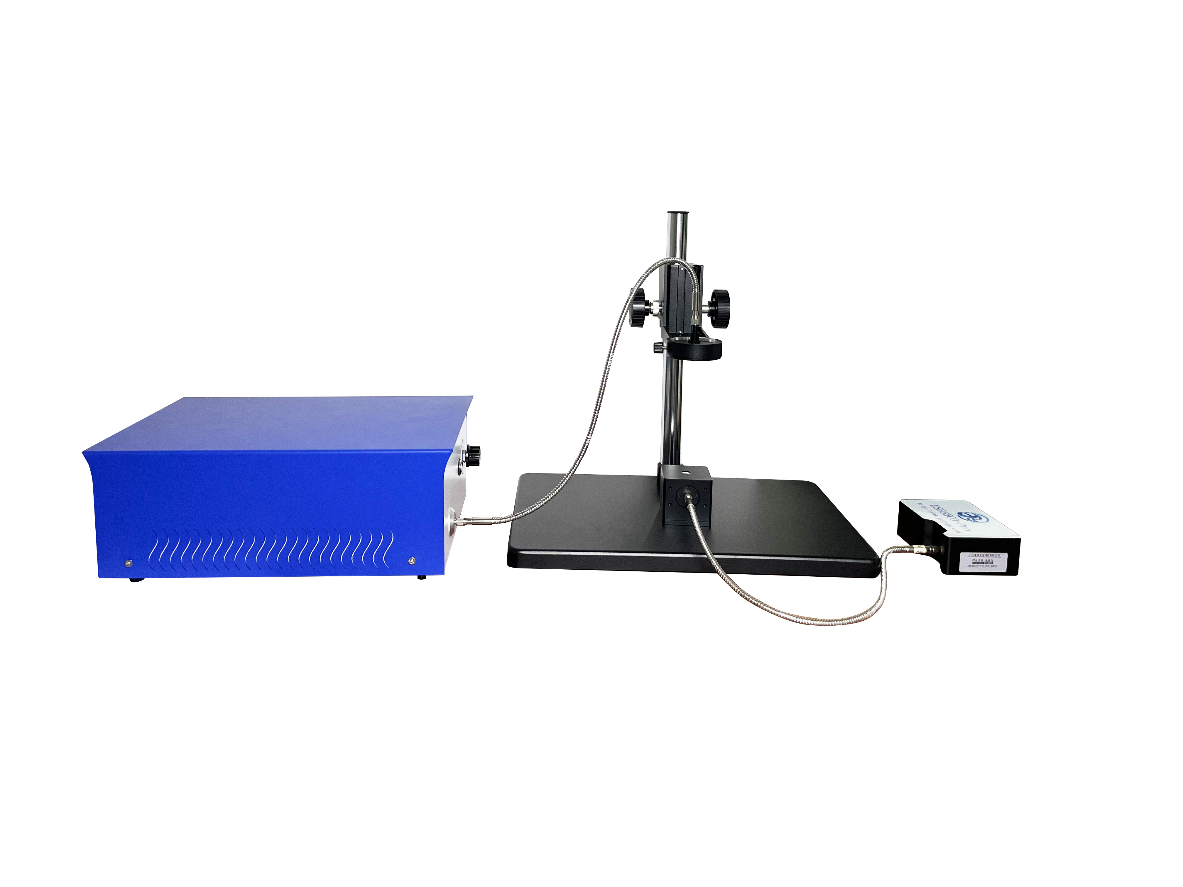
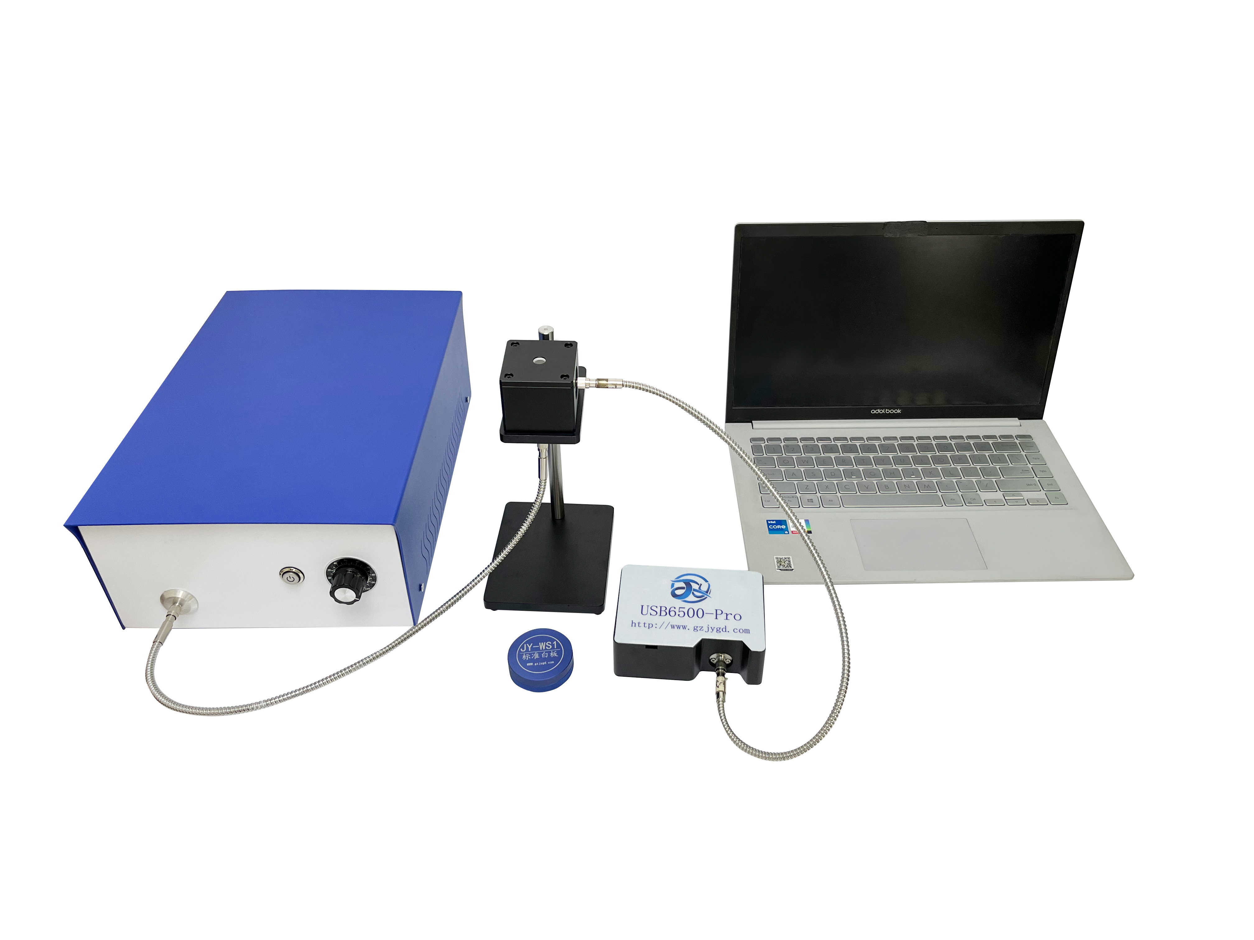
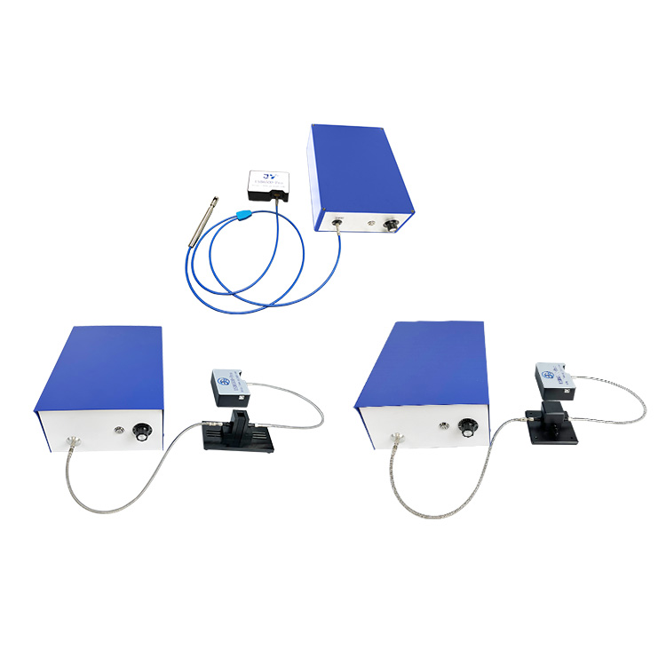
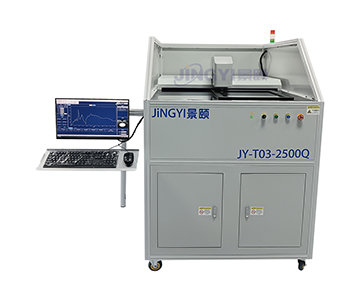
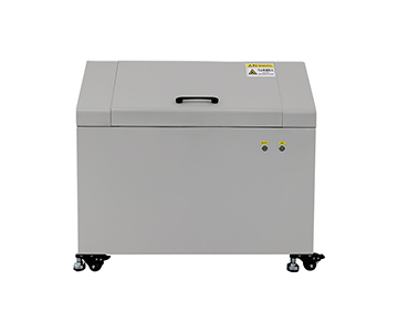
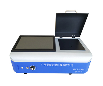
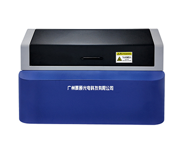
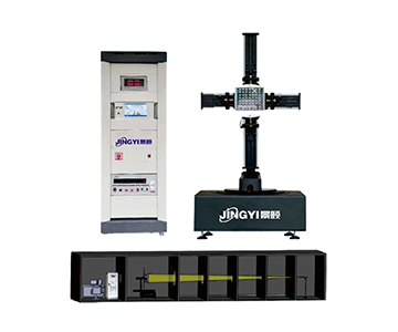
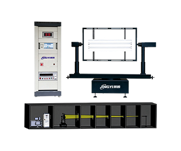
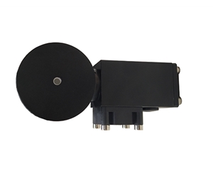
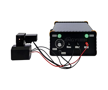
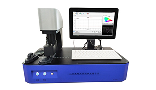
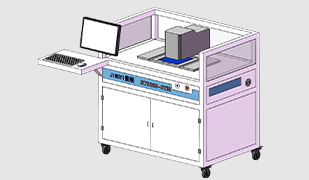
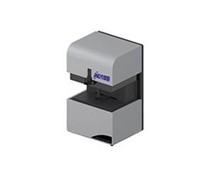
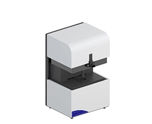
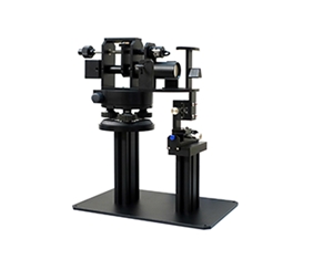
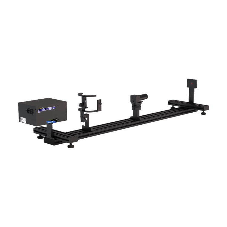
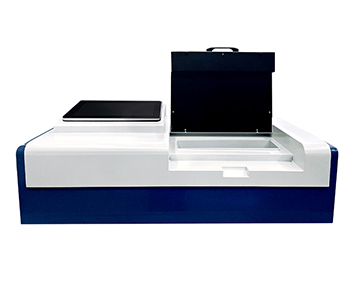
Reflectivity characterization forms the foundation for evaluating optical materials, coated components, and LiDAR targets. The product portfolio includes reflectivity meters, CHT-F03 model devices, reflectivity detection systems, and rearview mirror reflectivity testers. These serve three primary application clusters:
•Optical coating manufacturers conducting random inspection and uniformity analysis of film layer reflectivity.
•Semiconductor and optical communication device producers controlling surface reflection loss.
•Automotive rearview mirror and LiDAR target board reflectivity calibration.
Stable optical path design combined with standard whiteboard traceability maintains data consistency between production-line inspection and laboratory calibration.
Integrating Spheres
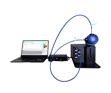
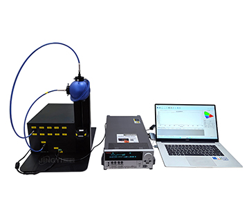
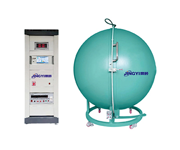
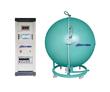
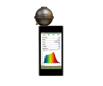
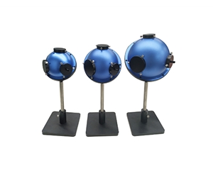
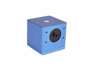
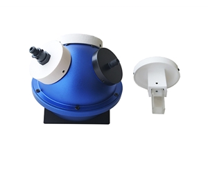
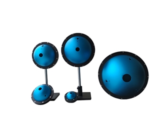
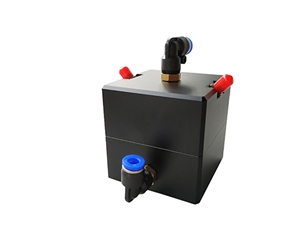
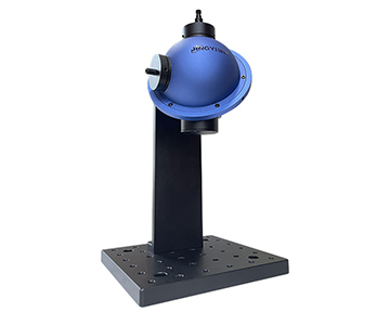
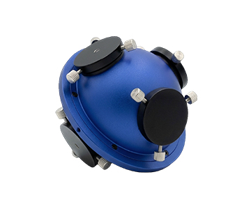
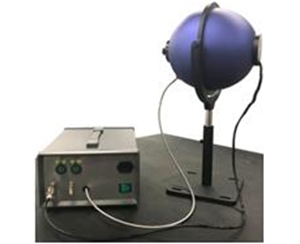
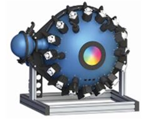
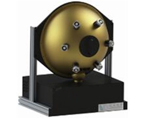
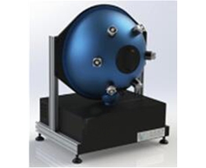
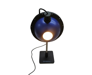
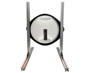
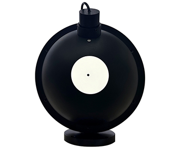
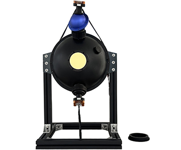
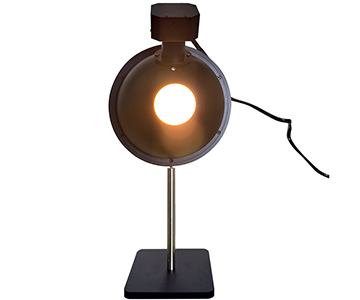
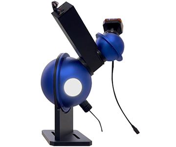
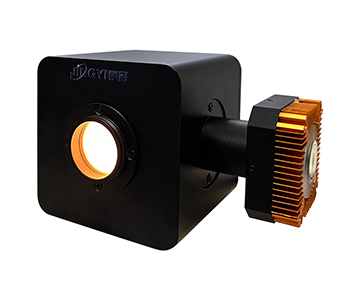
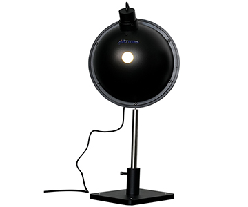
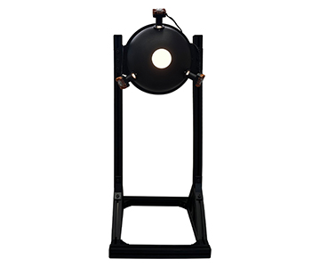
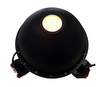
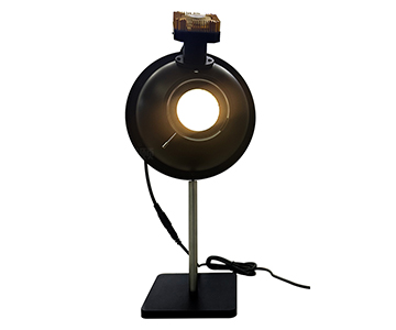
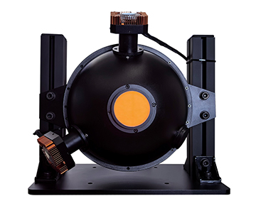
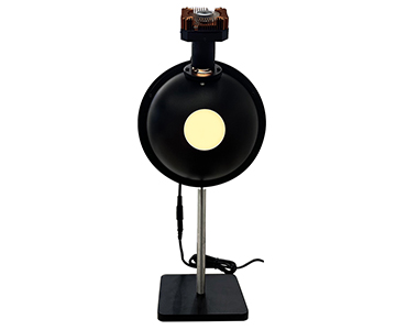
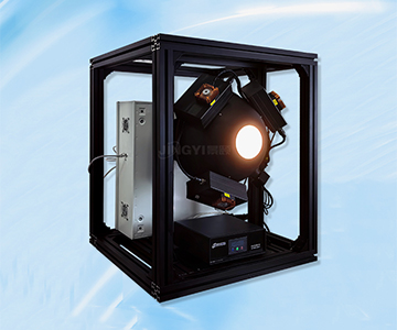
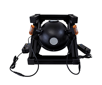
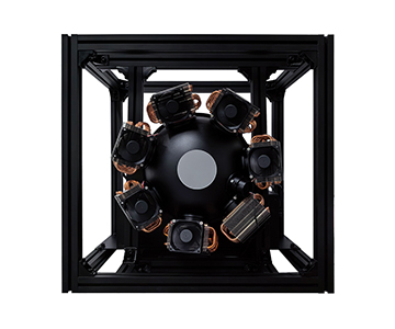
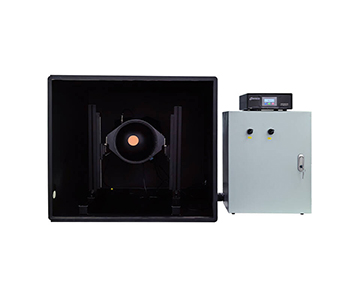
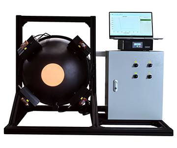
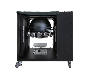
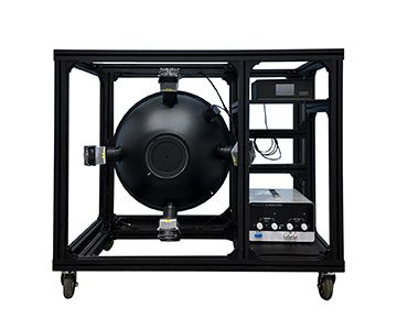
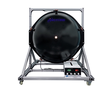
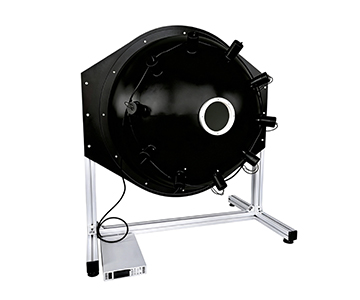
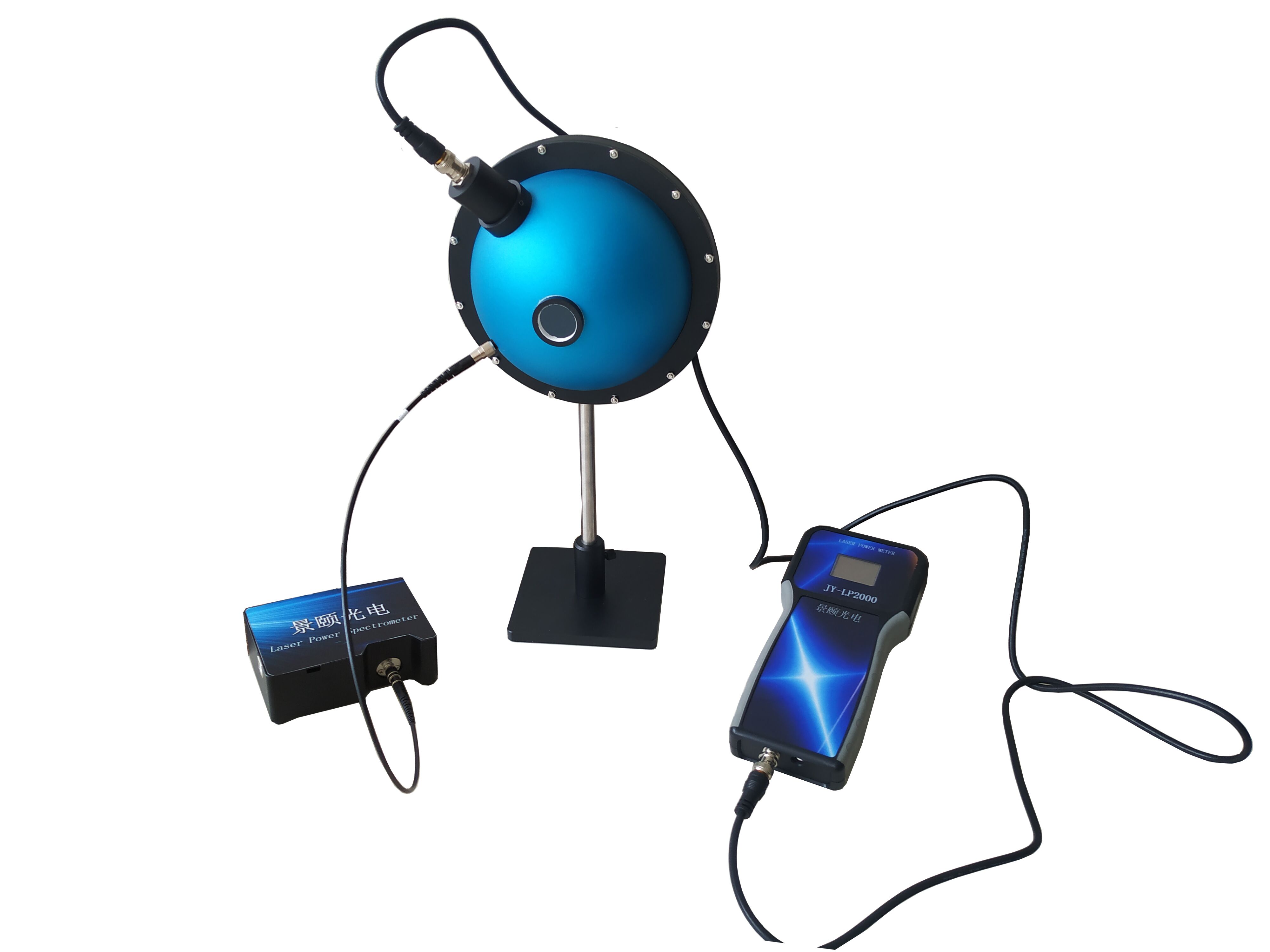
Integrating spheres collect diffuse reflected light, diffuse transmitted light, and source radiation signals—critical accessories in quantitative spectral measurement. The product range covers open integrating spheres, spheres with integrated light sources, custom-coated spheres, and gold-coated integrating spheres, spanning ultraviolet, visible, and near-infrared wavelength bands.
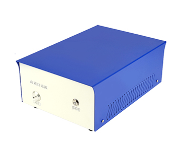
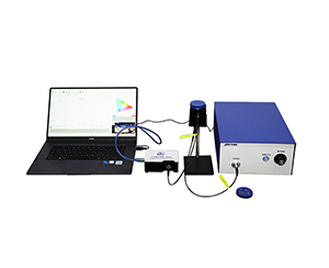
Customization and combinability define this segment: internal coating and port layout adjust to detector aperture, spectral range, and sampling method. When paired with spectrometers, light sources, and test software, complete measurement systems emerge for LED colorimetry, quantum efficiency measurement, laser power collection, and research-grade weak-light signal analysis.
Reflectance Panels
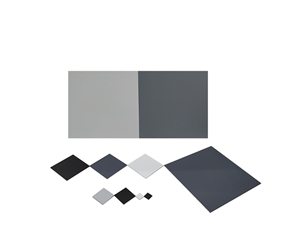
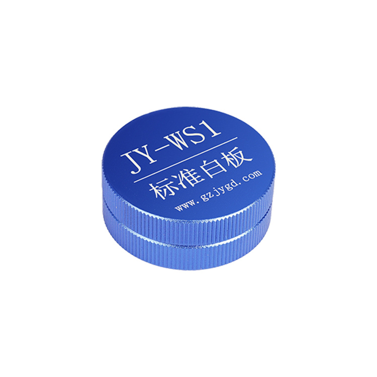
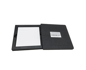
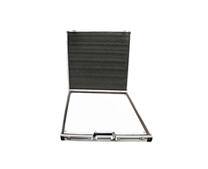
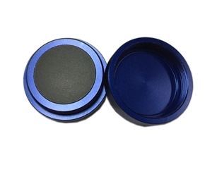
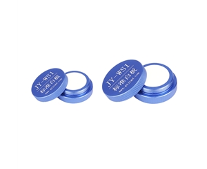
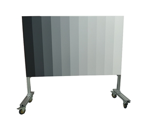
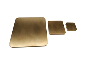
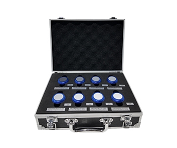
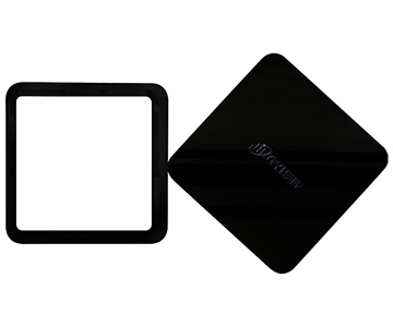
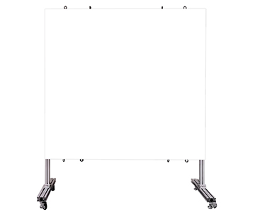
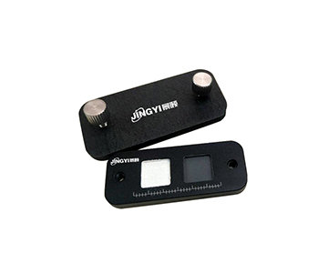
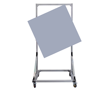
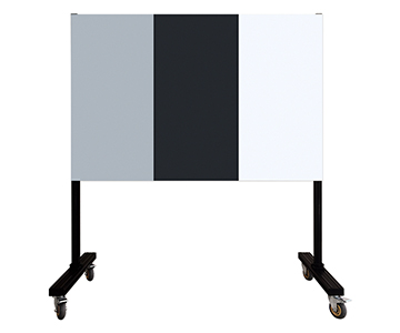
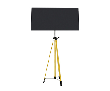
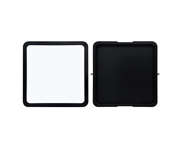
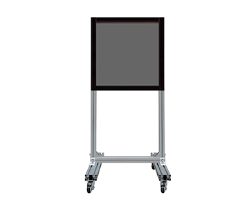
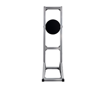
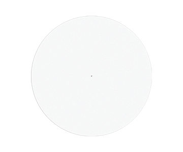
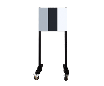
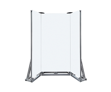
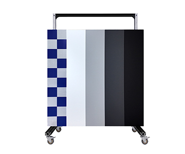
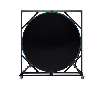
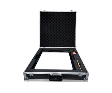
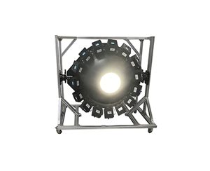
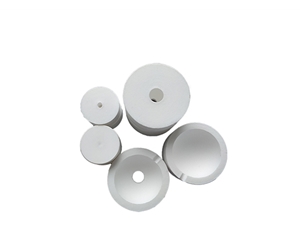
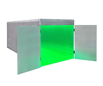
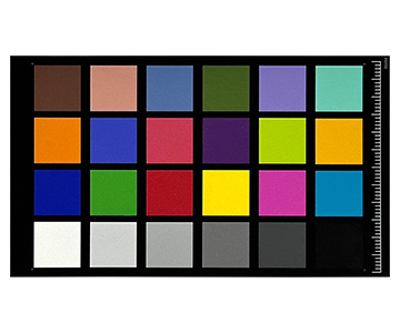
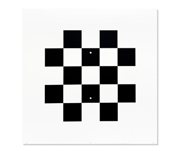
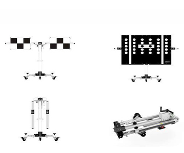
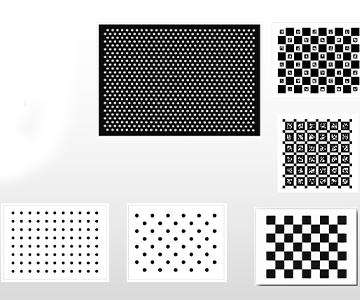
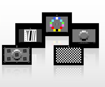
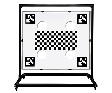
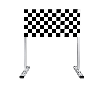
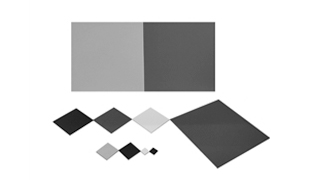
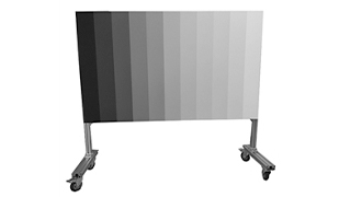
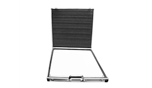
Reflectance panels serve as indispensable target references for LiDAR, cameras, and multispectral sensor calibration. The lineup includes LiDAR diffuse reflectance panels, standard whiteboards, automotive LiDAR calibration blackboards, and multi-level reflectivity拼接 panels (spliced panels), addressing measurement consistency across varying reflectivity intervals.
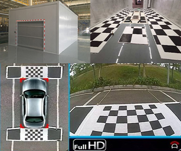
In LiDAR applications, panels support ranging calibration, point-cloud reflectivity validation, and target recognition testing. Machine vision and multispectral remote sensing scenarios rely on standard whiteboards for camera white balance and radiometric calibration. Autonomous driving test tracks use blackboards and拼接 panels to simulate low-, mid-, and high-reflectivity targets, validating perception algorithms under diverse environmental conditions.
Transmittance Measurement Instruments
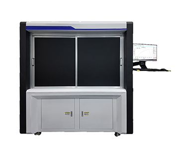
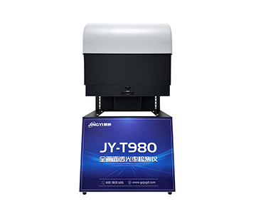
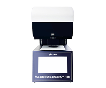
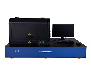
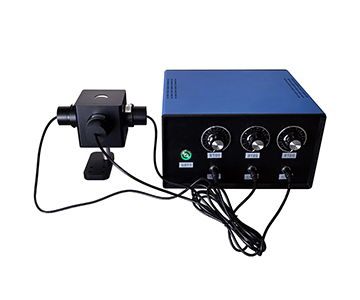
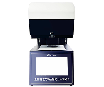
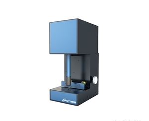
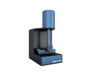
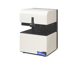
Transmittance detection targets glass, films, optical lenses, photovoltaic modules, and laser-welded materials. Semi-automatic transmittance testers, multi-point uniformity transmittance testers, photovoltaic glass transmittance testers, and fiber optic transmittance testers balance single-point measurement with area uniformity analysis.
Application requirements differ by sector: photovoltaic glass and encapsulation materials prioritize total transmittance and band-specific transmittance; plastic laser welding components demand spectral matching between transparent and absorbing layers; automotive and eyewear industries focus on selective transmittance across visible, infrared, and ultraviolet bands; optical communication devices require insertion loss and transmission stability at fiber end-faces. Spectral measurement replaces single-parameter judgment, better matching material R&D and production-line sorting needs.
Standards Participation and Industry Contributions
Jingyi Optoelectronics actively contributes to industry rule-making, feeding practical experience from equipment development back into standard documents. As a core drafting unit, the company has participated in the following standards:
| Standard No. |
Standard Name |
Role |
Application Field |
| T/CITS 231-2025 |
Technical Requirements for Automotive LiDAR |
Core drafting unit |
Automotive LiDAR, autonomous driving perception testing |
| T/WEA 089-2026 |
MEMS Micromirror for LiDAR |
Core drafting unit |
LiDAR micromirror components, automotive optical sensing |
| GB/T 47066-2026 |
Determination of Total Transmittance and Reflectivity of Plastics |
Core drafting unit |
Plastic optical materials, packaging and functional film inspection |
| T/CIET 2298-2026 |
Calibration Specification for Thin Film Interference Thickness Measurement Systems |
Core drafting unit |
Optical coating, semiconductor thin film thickness measurement |
| T/CWDPA 136-2026 |
Performance Evaluation of AI-Driven Spectral Analysis Algorithms for UV-Visible Fiber Spectrometers |
Core drafting unit |
Spectrometer algorithm evaluation, intelligent detection, optical communication analysis |
These standards span “LiDAR system—core MEMS mirror—material transmittance/reflectivity—film thickness calibration—spectral algorithm evaluation” layers. Participation translates into earlier understanding of industry test boundaries during product development: which parameters require traceability, which errors demand quantification, and which scenarios need unified evaluation criteria.
In automotive LiDAR, reflectivity characteristics, ranging capability, and test panel consistency directly impact point-cloud evaluation results. In plastics and films, total transmittance and reflectivity test methods determine optical performance comparability. Jingyi Optoelectronics maps test logic from standards into reflectivity meters, integrating spheres, and transmittance instruments, aligning equipment output with industry-standard language.
Strategic Value of the Shantou R&D Center
Value to the Enterprise
•R&D collaboration efficiency: Shantou center absorbs application validation and custom development, creating division of labor with Guangzhou headquarters and shortening requirement-to-prototype cycles.
•Technical system completeness: Strengthens optical algorithms, environmental adaptability design, and automated test software, pushing equipment from “capable of measuring” to “traceable, repeatable, batch-ready.”
•Innovation credential accumulation: Expanded R&D system clarifies technical evidence chains for R&D expense management, IP layout, and science-technology project applications, laying groundwork for higher-level qualification filings.
•Talent and scenario co-evolution: Proximity to regional manufacturing and university resources feeds semiconductor, new energy, and optical coating customer problems back into product planning, reducing information loss between R&D and field application.
Value to Customers
•Verifiable technical reliability: Standards participation signals systematic understanding of test conditions, error sources, and traceability—customers receive not just instruments but explainable measurement methodologies.
•Enhanced service continuity: Parallel R&D centers improve response speed for custom projects, algorithm upgrades, and production-line retrofits, critical for iterative optical inspection scenarios.
•Reduced compliance and integration costs: Equipment test methods aligned with industry standards lower data communication costs during supplier audits, production-line acceptance, and cross-laboratory comparisons.
•Domestic supply stability: In high-end optical inspection, imported equipment often suffers long lead times, high maintenance costs, and slow customization response. A localized R&D expansion offers替代 solutions closer to domestic production habits, improving supply chain resilience.
Shantou R&D Center Team Profile
The Shantou facility is anchored by a 28-member core team drawn from the company’s existing talent pool and regional recruitment, with disciplinary coverage spanning optical engineering, precision mechanical design, embedded electronics, measurement algorithm development, and industrial software. Team composition reflects the “>50% R&D staff” ratio maintained across all Jingyi Optoelectronics sites.
Key leadership includes a principal optical architect with 14 years in spectroscopic system design (previously at a tier-1 German metrology equipment manufacturer), a mechanical engineering lead specializing in thermal-stable structures for integrating spheres, and an algorithm group manager focused on AI-driven spectral analysis optimization. The team operates in two-track mode: one track dedicated to custom application engineering for semiconductor and LiDAR customers, the other to standards-compliant product platform iteration.
Collaboration protocols between Shantou and Guangzhou include weekly technical synchronization, shared simulation environments for optical path modeling, and a joint design-review process that routes all production-intent changes through both sites before release. This structure ensures that field-derived requirements from semiconductor fabs in the Pearl River Delta and optical coating plants in southern China are processed within 72 hours into actionable engineering tasks.
Semiconductor Manufacturing Applications
In semiconductor manufacturing, spectroscopic detection and optical measurement address critical pain points across wafer fabrication and advanced packaging:
•Thin-film thickness calibration: At a GaN device fabrication facility in southern China, the evaluated system reduced film thickness measurement variance by 37.2% compared to a legacy contact profilometer when monitoring ALD-deposited high-k dielectric layers (sample size: n=84 wafers, measured at 23°C ±1°C). The non-destructive optical approach eliminated wafer contact damage and supported in-line sampling every 25 wafers.
•Reflectivity loss control on optical couplers: A photonic chip packaging line integrated reflectivity meters to qualify laser-to-fiber coupling surfaces, cutting coupling loss variability from ±0.8 dB to ±0.3 dB across a 3-month production run (n=12,000 devices). Stable optical path design with standard whiteboard traceability enabled direct data comparison between incoming inspection and final test stations.
•Wafer-level transmittance screening: For silicon photonics wafers requiring band-specific infrared transmittance validation, a multi-point uniformity transmittance tester identified edge-of-wafer coating defects that a single-point sampling method missed, improving yield prediction accuracy by 22% during a 6-week pilot (n=18 wafers per lot, 5 lots evaluated).
These cases illustrate how measurement repeatability, traceability, and speed translate into quantifiable yield and cost improvements on the production floor.
Future Development Roadmap
•Technical breakthroughs: Increased R&D investment in sub-nanometer film thickness measurement, low-illumination integrating detection, and multi-gradient reflectivity calibration for LiDAR, targeting measurement stability under complex scenarios.
•Product expansion: Extending the spectroscopic detection portfolio to include beam profiling, attenuator calibration, quantum efficiency systems, and inline optical inspection components.
•Import substitution: Advancing the steady replacement of imported high-end reflectivity, transmittance, and integrating sphere measurement systems, focusing on traceability architecture, software usability, and long-term consistency.
•Standards leadership: Continuing participation in national and group standards, codifying experience from automotive LiDAR, optical films, and spectral algorithm evaluation into public test methods.
•Scenario deepening: Delivering “instrument + calibration panel + software + methodology” bundled services to semiconductor manufacturing, optical communication, new energy, and research institutions, moving beyond single-hardware delivery.
About Jingyi Optoelectronics
Jingyi Optoelectronics is a Guangzhou-based high-tech enterprise focused on R&D, production, and service of spectroscopic detection and optical precision measurement equipment. The company’s main products include reflectivity detectors, vision calibration panels, integrating spheres, fluorescence quantum efficiency detection systems, and custom measurement solutions. Business coverage spans semiconductor manufacturing, optical communication, LiDAR, optical coating, new energy, and research institutions.
Leveraging collaborative R&D foundations in Guangzhou, Beijing, and Shantou, Jingyi Optoelectronics has built an end-to-end system from optical design, mechanical structure, and electronic control to spectral algorithms and test software. Customization extends to sample form, wavelength range, and production-line cycle. Core products support on-site modification of ports, coatings, dimensions, and communication interfaces. The company’s value proposition centers on “accurate measurement, traceability, reusability”—translating standards participation into engineering implementation through R&D centers and controlled production environments. For customers requiring import substitution, production-line upgrades, or research calibration, the firm provides support from single instruments to system-level solutions.
Frequently Asked Questions
Q1: What measurement uncertainties can be expected from spectroscopic reflectivity systems in production environments?
A: Under controlled conditions (23°C ±2°C, 45–65% RH), repeatability of ±0.15% reflectivity has been documented across 200 measurement cycles on calibrated reference panels. Production-floor performance may vary with vibration and thermal drift; environmental isolation measures are recommended for sub-0.2% stability.
Q2: How do integrating sphere coatings affect measurement accuracy across UV to NIR ranges?
A: Coating selection determines spectral flatness and diffuse reflectance uniformity. PTFE-based coatings offer >98% reflectivity from 400–1500 nm but degrade below 300 nm. Gold coatings extend to mid-IR but introduce spectral structure. Matching coating to application wavelength is critical—mismatched coatings can introduce 2–5% systematic error.
Q3: What calibration intervals are recommended for LiDAR reflectance panels?
A: For panels used in automotive-grade LiDAR validation, recalibration every 6 months or 500 exposure hours (whichever comes first) maintains traceability to NIST-referenced standards. Field conditions with high UV exposure or abrasive cleaning may require 3-month intervals.
Q4: Can transmittance measurement systems handle curved automotive glass samples?
A: Yes, with custom fixturing. The optical path must account for refraction at curved surfaces; specialized sample holders maintain consistent angle of incidence. Measurement variance on curved samples is typically 0.3–0.5% higher than on flat references of identical material.
Q5: How can I independently verify the accuracy of a delivered optical thickness gauge before accepting a purchase order?
A: Request a factory acceptance test (FAT) protocol using NIST-traceable reference wafers with certified thickness values across the measurement range. Conduct on-site validation with at least three known standards spanning low/mid/high reflectivity. Compare results against a previously qualified system or third-party metrology lab report. Document all conditions: temperature, humidity, sample preparation, and measurement location on the wafer.
About This Guide
Data Sources
: T/CITS 231-2025, T/WEA 089-2026, GB/T 47066-2026, T/CIET 2298-2026, T/CWDPA 136-2026 standards texts; in-house validation reports (n=84 wafers for film thickness; n=12,000 devices for coupling loss); SEMI PV22-0715 public reference.
Author
: Cai Xiaodong, Senior Application Engineer, Jingyi Optoelectronics, 9 years in optical metrology and spectroscopic system integration.
Disclosure
: Jingyi Optoelectronics manufactures spectroscopic detection and optical precision measurement equipment. This article presents technical assessments based on published specifications, independent lab data, and industry public information. No compensation was received from third-party brands mentioned.
Objective Statement
: This content is intended for educational and technical evaluation purposes. Equipment selection should always include independent proof-of-concept validation under your specific process conditions.
Last Updated
: October 2026
For detailed specifications and application notes on spectroscopic detection systems, search "Jingyi Optoelectronics optical measurement" or visit our technical library.