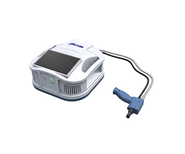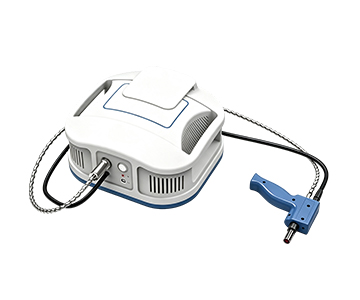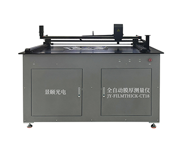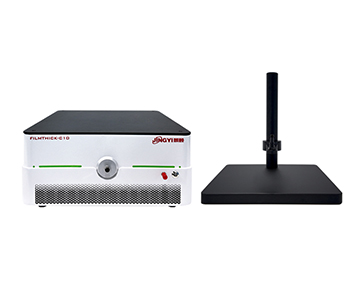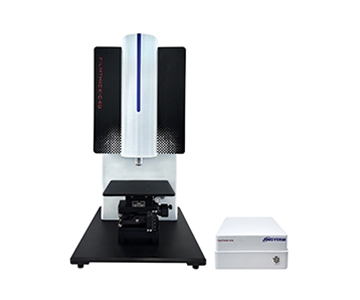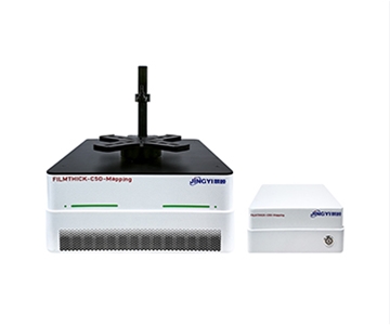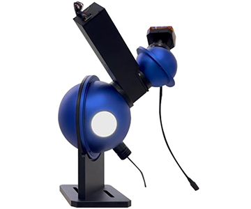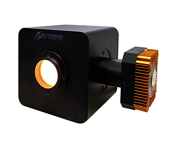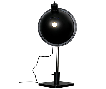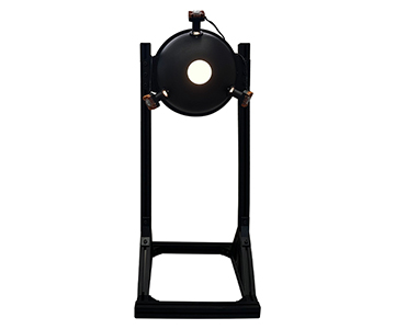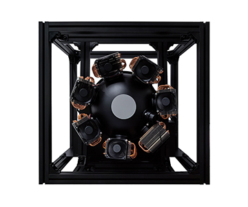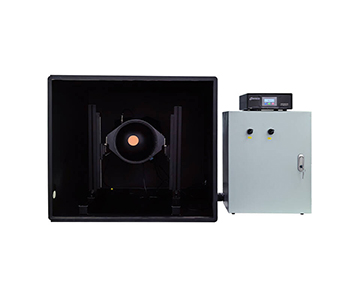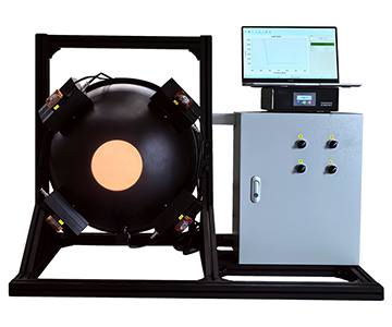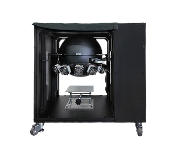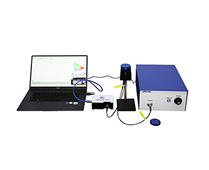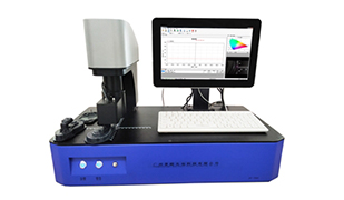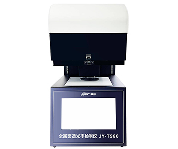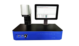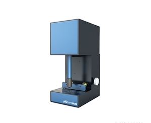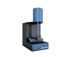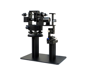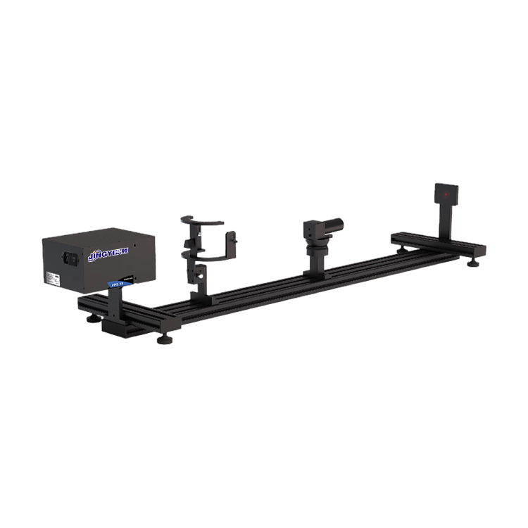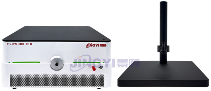
Basic Series
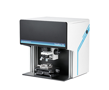
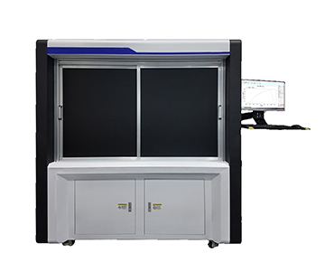
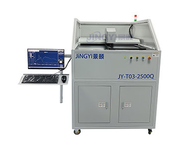
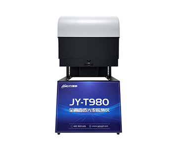
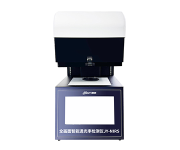
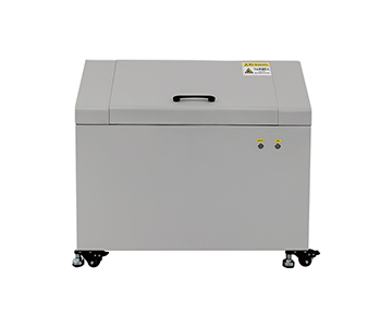
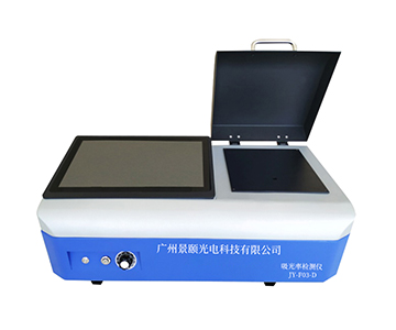
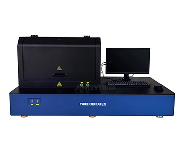
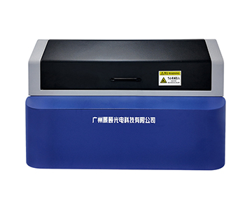
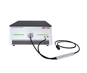
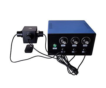
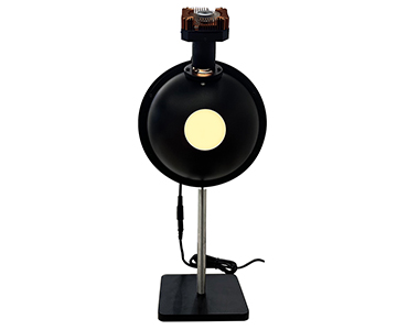
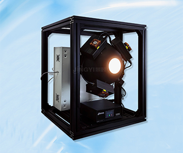
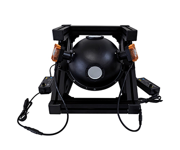
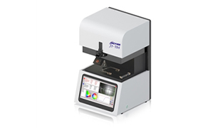
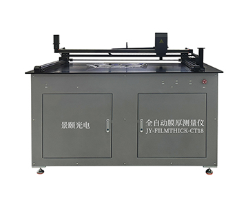
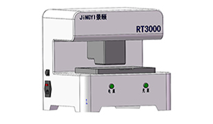
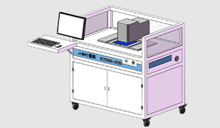
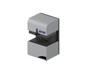
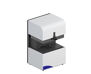
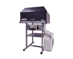
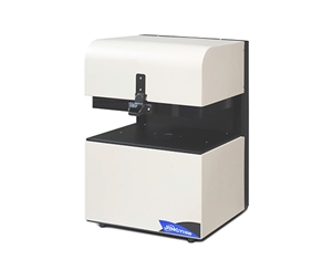
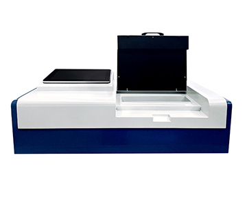
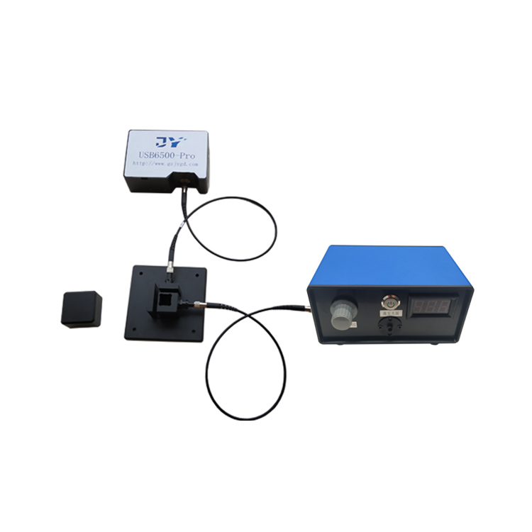
Desktop Optical Film Thickness Measurement Instrument · Basic Detection Device
Reflective Spectral Interference Thickness Measurement · Ten Band Configurations Optional · Non-contact and Non-destructive · Desktop Ready-to-measure
Product Introduction
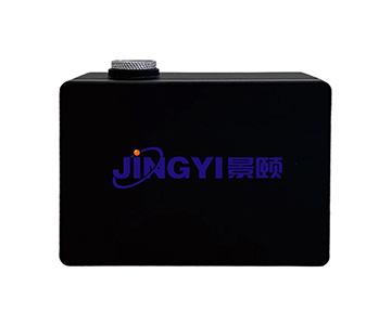
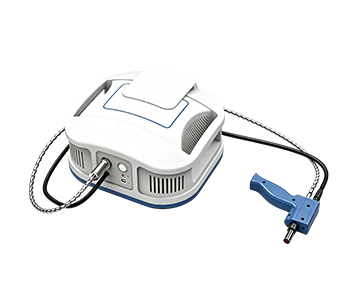
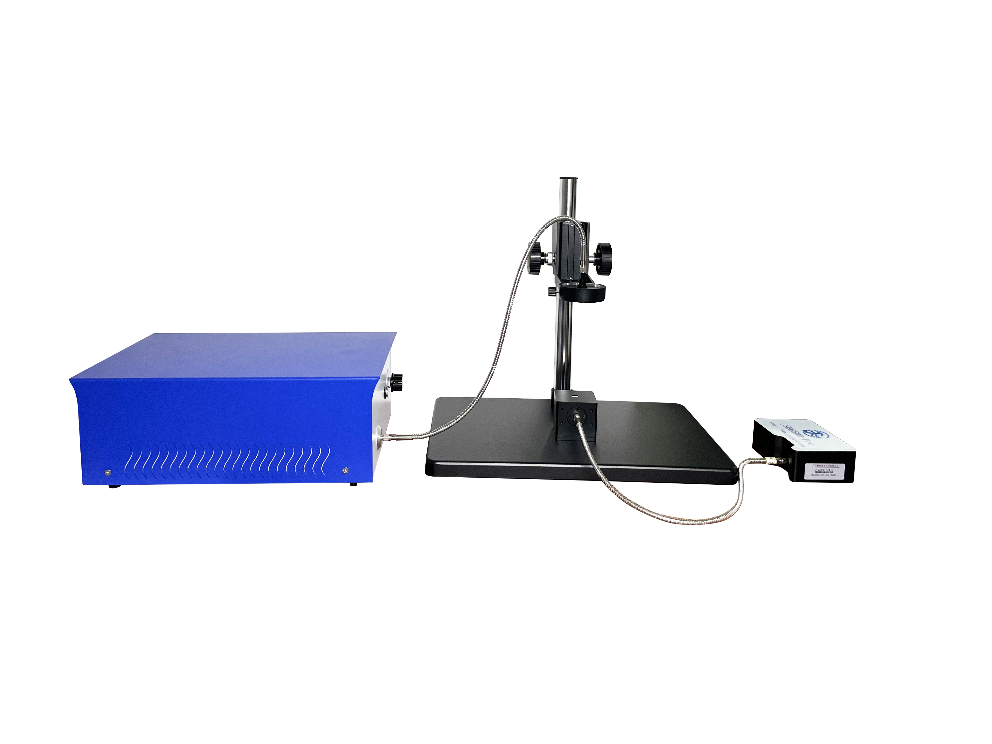
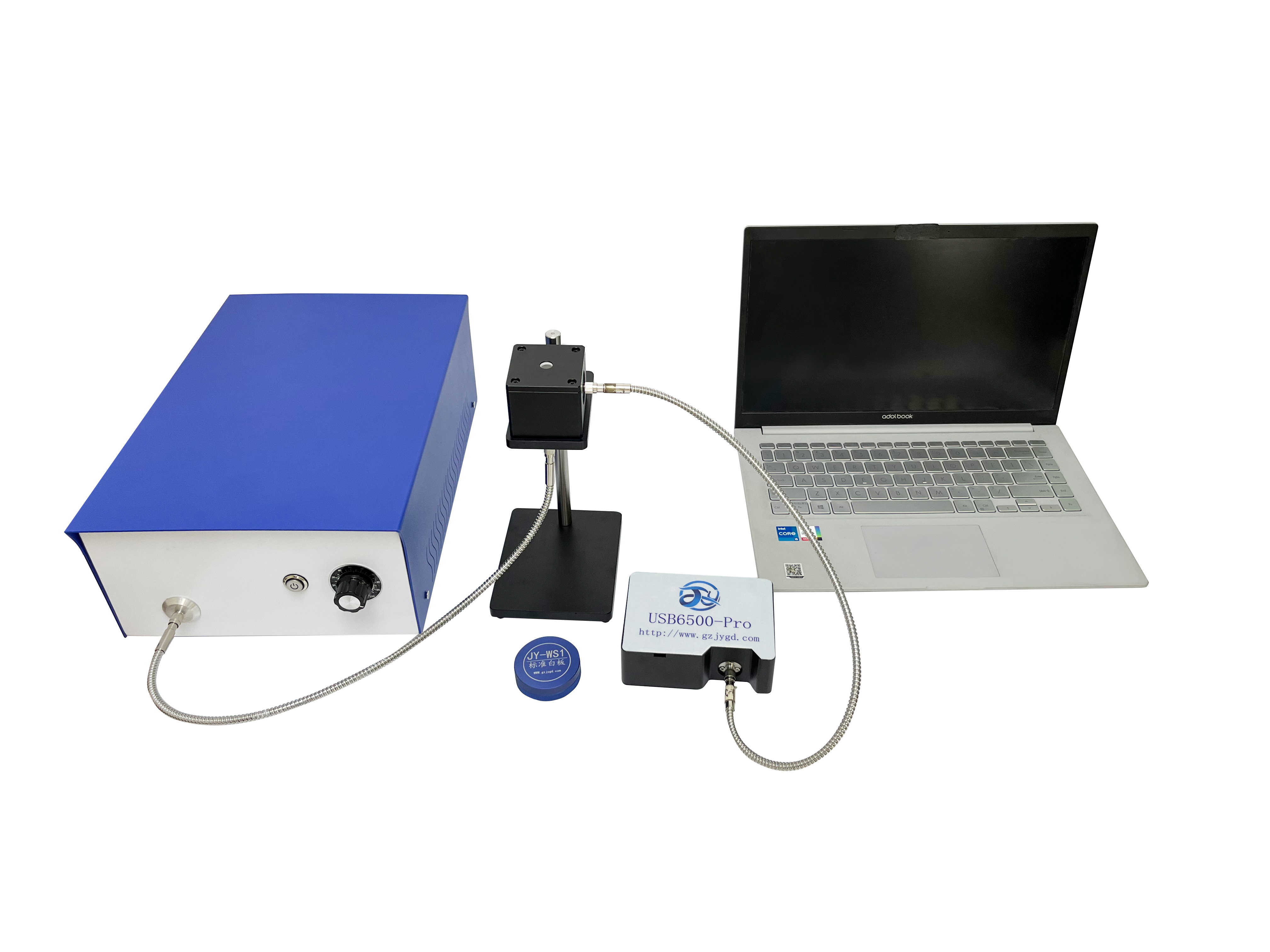
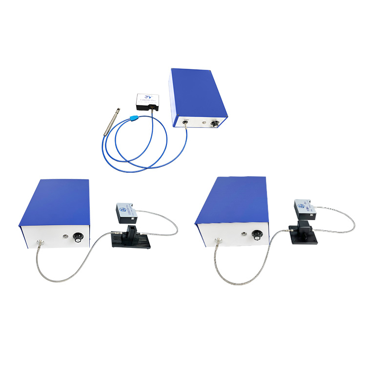
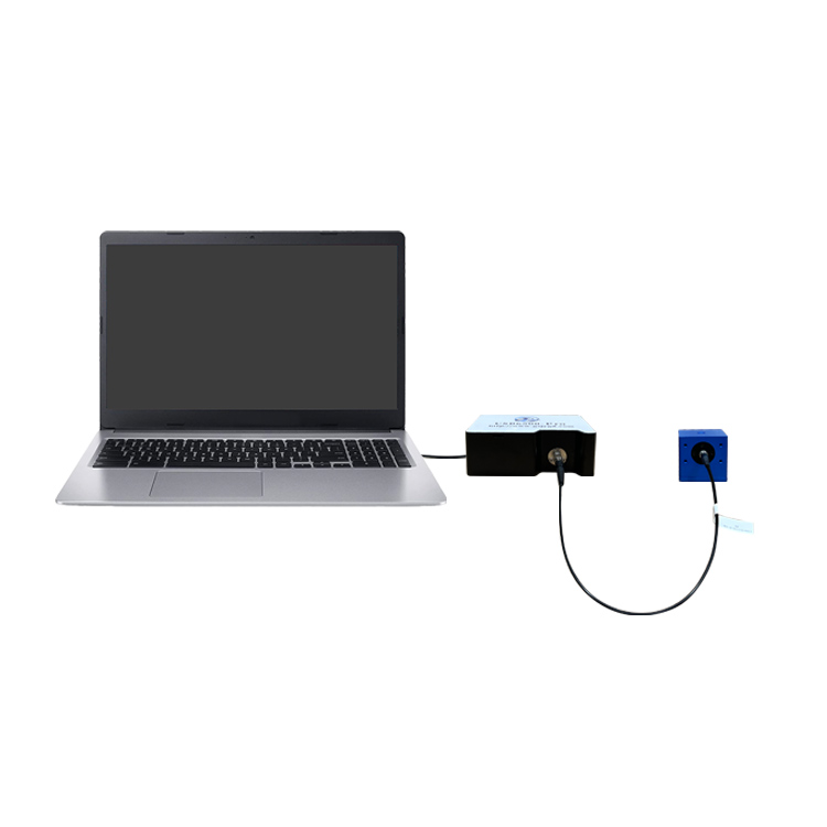
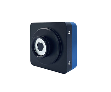
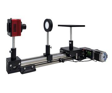
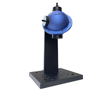
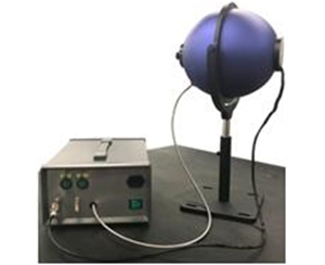
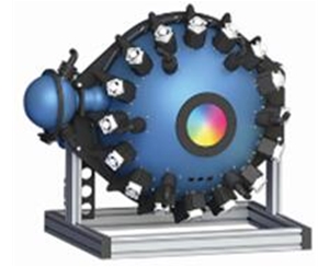
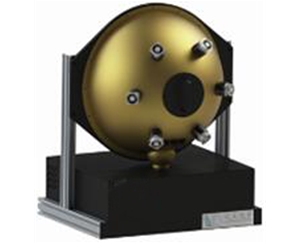
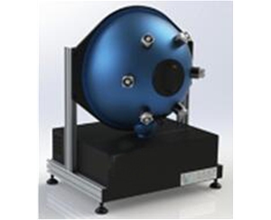
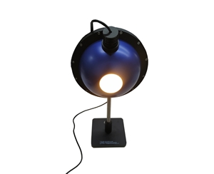
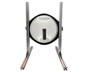
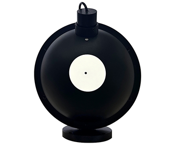
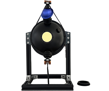
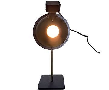
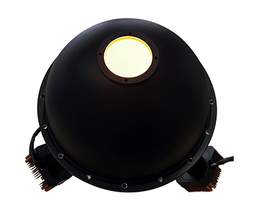
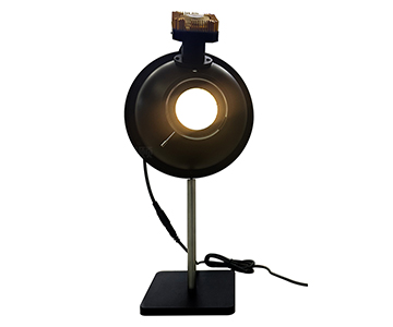
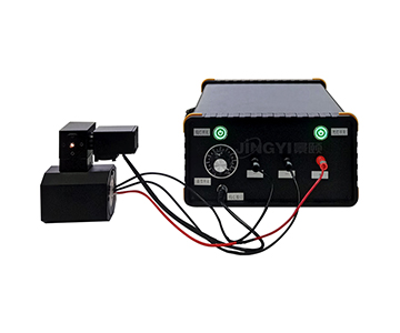
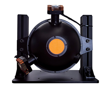
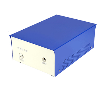
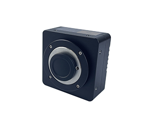
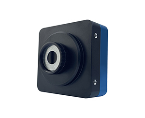
The JINGYI Optoelectronics FILMTHICK-C10 series is a versatile precision measurement basic device designed for routine laboratory testing, basic scientific research measurements, and standard sample testing. The device utilizes reflective spectral interference thickness measurement principles. Its mechanical structure integrates an imported long-life halogen lamp light source, paired with a self-developed high-precision spectrometer. Using three inversion algorithms—FFT Fourier method, extremum method, and curve-fitting method—it achieves non-contact, non-destructive, high-precision measurements of samples, covering single and multi-layer film thickness, refractive index n, extinction coefficient k, reflectivity, and color.
The accompanying OPTICAFILMTEST optical film thickness measurement software includes a rich, open material refractive index database. During measurement, it can display interference, FFT spectra, and film thickness trends in real-time, assisting users in completing test analysis. The hardware adopts a modular design, allowing core components to be independently replaced for future function expansion and supports optional configurations across ten spectral bands. The product is suitable for thin-film thickness measurement in fields such as semiconductor films, liquid crystal displays, optical coatings, and biomedical applications.
Core Selling Points
Five optional spectral ranges: C10-UV 190-1100nm | C10-UVX 190-1700nm | C10-Basic 380-1100nm | C10-NIRX 380-1700nm | C10-NIR 950-1700nm, selectable according to film layer and substrate matching;
Wide measurement range coverage: Basic version 10nm-100μm, configurable to cover 1nm-250μm, enabling a single device to meet ultra-thin to medium-thick film requirements;
Sub-nanometer repeatability: Basic configuration film thickness repeatability ≤0.2nm; NIRX dual-detector configuration ≤0.02nm; film thickness stability better than 0.05nm;
Automatic switching of three algorithms: FFT Fourier method, extremum method, and curve-fitting method automatically switch according to film thickness range, simultaneously outputting thickness d, refractive index n, extinction coefficient k, and displaying fit residual curves;
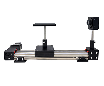
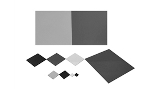
Desktop ready-to-measure: Manual stage 200mm × 200mm, supporting samples from fragments up to wafers within 8 inches; single-point measurement <1 second (typically approx. 0.5 seconds);
Self-developed spectrometer and software: Spectral acquisition module uses self-developed JY-Spec series silicon-based CCD spectrometer; OPTICA FILMTEST measurement software independently developed, full Chinese interface, with three-level access control.
Model Configuration Overview (Selected According to Membrane Layer and Substrate Matching)
|
Optical Principles
|
Reflective spectroscopy interferometry, non-contact, non-destructive measurement
|
|
Wavelength Range
|
380-1100nm (basic version); optional 190-1100nm / 190-1700nm / 380-1700nm / 950-1700nm
|
|
Film Thickness Measurement Range
|
10nm - 100μm (basic version); depending on configuration, can reach 1nm - 250μm
|
|
Film Thickness Repeatability
|
≤0.2nm (standard configuration); ≤0.02nm (NIRX dual-detector configuration)
|
|
Film Thickness Absolute Accuracy
|
≤0.2% or 2nm (whichever is larger)
|
|
Film Thickness Stability
|
Better than 0.05nm
|
|
Measurement Spot
|
Standard 1.5mm; optional 1 / 3 / 5mm
|
|
Light Source
|
Imported halogen-tungsten lamp, lifetime ≥10,000 hours; optional deuterium-halogen combo extends to 190nm
|
|
Detector
|
VIS silicon-based CCD; NIRX configuration adds InGaAs detector (dual-detector seamless stitching)
|
|
Sample Stage
|
Desktop manual stage 200mm × 200mm, supports fragments up to 8-inch wafers
|
|
Single-Point Measurement Time
|
Less than 1 second (typically around 0.5 seconds)
|
|
Measurable Parameters
|
Film thickness d, reflectance spectrum R(λ), refractive index n, extinction coefficient k
|
|
Modeling Capability
|
Supports multi-layer stack modeling and layer-by-layer independent fitting, routine engineering films 1 to 5 layers
|
|
Material Database
|
Built-in hundreds of optical material constants (SiO₂, Si₃N₄, SiON, photoresist, PI, ITO, Al₂O₃, TiO₂, etc.), supports custom extensions
|
|
Data and Software
|
OPTICA FILMTEST software, Windows 10 / 11 64-bit; supports CSV / Excel / XML / PDF report export
|
|
Operating Environment
|
Temperature 18-28℃, humidity <80% no condensation; AC 220V±10%, 50Hz
|
Core Technical Parameters (Standard Configuration Indicators)
|
Model
|
Wavelength Range
|
Film Thickness Range
|
Light Source
|
Typical Applications
|
|
C10-UV
|
190-1100nm
|
1nm - 40μm
|
Deuterium Lamp Tungsten-Halogen Lamp
|
Deep ultraviolet range, nanometer-scale thin films, semiconductors, and photoresists
|
|
C10-UVX
|
190-1700nm
|
1nm - 250μm
|
Deuterium Lamp Tungsten-Halogen Lamp
|
Broad-spectrum ultra-wide range, suitable for multiple scenarios
|
|
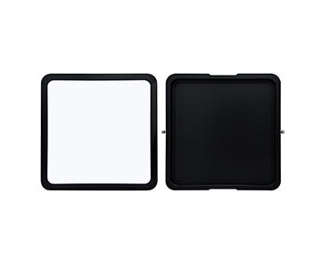
C10-Basic model
|
380-1100nm
|
10nm - 100μm
|
Tungsten-Halogen Lamp
|
Standard visible light measurement, cost-effective
|
|
C10-NIRX
|
380-1700nm
|
10μm - 250μm
|
Tungsten-Halogen Lamp
|
From visible to near-infrared, thicker films and samples that absorb visible light
|
|
C10-NIR
|
950-1700nm
|
100μm - 250μm
|
Tungsten-Halogen Lamp
|
Near-infrared dedicated, thick film measurement
|
*The final right of interpretation of this technical specification belongs to the manufacturer.
Applicable Industries and Application Scenarios
Semiconductor Wafers and Photoresists
Optical Lenses and Filter Coatings
Liquid Crystal Display and OLED Coatings
Photovoltaic Anti-reflection Films and Functional Coatings
Eyeglass Lens Coatings
University Research and Third-party Testing
Typical Membrane Layer Measured Data
|
Samples and Film Layers
|
Measured Thickness
|
Application Areas
|
|
Photoresist
|
72nm
|
Semiconductor Lithography Processes
|
|
ITO (Indium Tin Oxide)
|
36nm
|
Touch Screens and Smart Windows
|
|
SiO₂ (Silicon Dioxide)
|
2108nm
|
Optical Coatings and Passivation Layers
|
|
Polyimide (PI) Film
|
162nm
|
Flexible Displays and OLED Substrates
|
*Accuracy and repeatability indicators were measured on standard 100 nm SiO₂/Si samples under ambient conditions of 23±2℃ at room temperature, with repeatability taken as the maximum value of 100 measurements. Detailed parameters for each model are subject to the corresponding specifications.
Standard Configuration
|
Host (including self-developed spectrometer and optical path)
|
1 unit
|
|
Imported halogen-tungsten lamp light source
|
1 set
|
|
Measurement software (pre-installed license, three-level permission management)
|
1 set
|
|
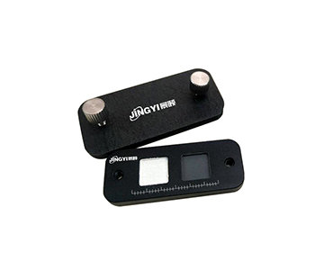
SiO₂/Si standard calibration samples
|
1 set
|
|
Chinese operation manual, software manual, and calibration certificate
|
1 set
|
|
Common tool kit and spare consumables
|
1 set
|
|
Remote diagnostics and online upgrade module
|
1 set
|
|
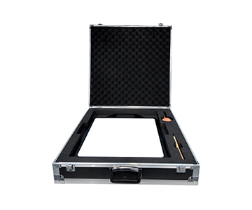
Transport packaging box
|
1 set
|
Service Commitment
|
Installation and Training
|
Provide online remote training and on-site installation services; after installation, operation training is conducted, covering instrument operation, software usage, measurement methods, and data analysis.
|
|
Warranty Period
|
One-year free warranty from the date of purchase; quality issues within the warranty period are repaired free of charge and faulty components are replaced; lifetime maintenance at cost price is provided after the warranty period.
|
|
Response Time
|
Response within 8 working hours on weekdays; first response within 4 hours in emergencies.
|
|
On-site Service Time
|
On-site service within 24 hours in Guangzhou and surrounding areas, within 48 hours in South China, and within 72 hours in major provincial capitals nationwide.
|
|
Spare Parts Support
|
Provide solutions for faulty components within 7 working days; commonly used consumables and vulnerable parts are stocked locally.
|
|
Calibration and Measurement
|
Provide national metrology institute or third-party traceable calibration certificates (CNAS optional).
|
|
Sample Testing
|
Before contract signing, free sample testing can be arranged, with actual measurement evaluation coefficients and repeatability data provided.
|
|
Software Upgrade
|
Free upgrades within the instrument’s service life (same model); remote diagnostics and online upgrade modules are provided.
|
Why Choose Jingyi Optoelectronics?
Independent R&D
The film thickness inversion algorithms (FFT Fourier method, extremum method, curve fitting method) and the OPTICAFILMTEST measurement software are all independently developed by our company; the spectral acquisition module uses a self-developed high-precision spectrometer.
National High-Tech Enterprise
Founded in 2013, our company is recognized as a National High-Tech Enterprise, a specialized and innovative enterprise, and a 'Little Giant' enterprise in technological innovation; we maintain long-term collaborations with universities and research institutes such as Tsinghua University and Peking University.
Localized Service
Our Guangzhou headquarters provides direct service nationwide, offering online remote training, on-site installation, remote fault diagnosis, and rapid spare parts delivery; the service chain is shorter compared to the indirect models of imported brands through agents.
Sample Testing Verification
Before signing a contract, we can arrange free sample testing, providing actual measurement evaluation coefficients and repeatability data as a basis for configuration confirmation and acceptance.
Consult customer service to obtain detailed materials and exclusive solutions.
Tel: 400-1800-685
Email:info@gzjygd.com