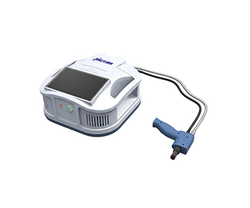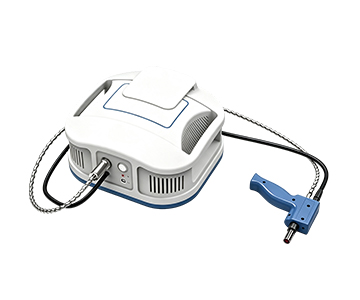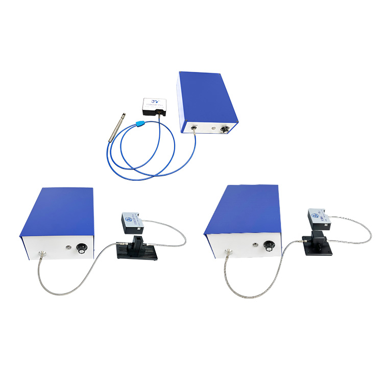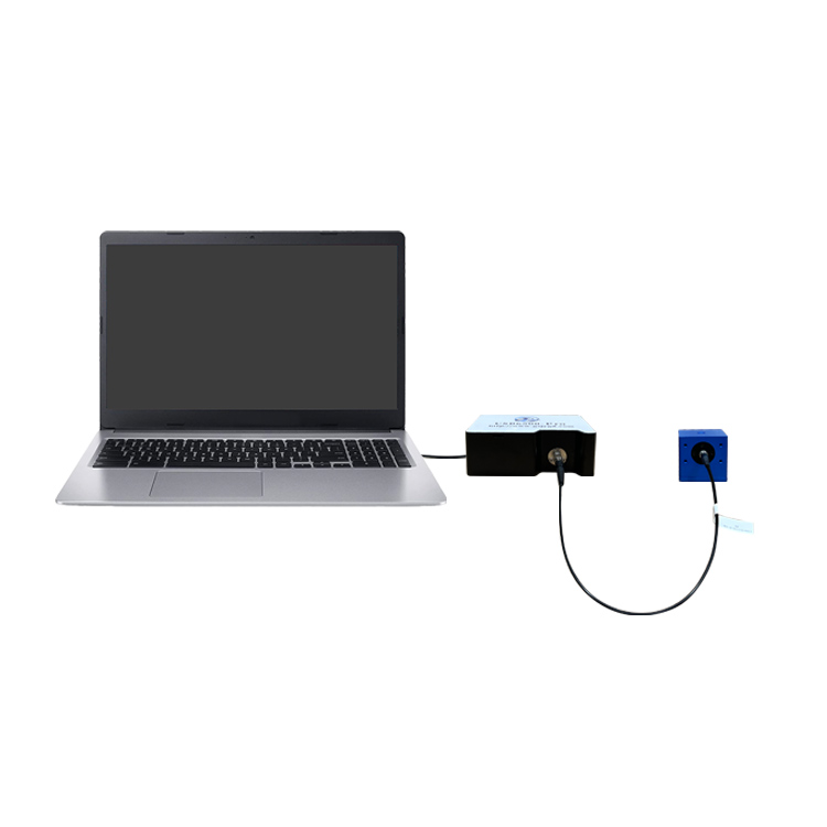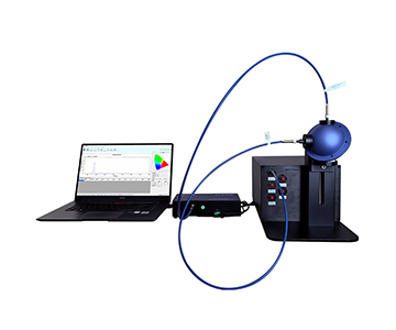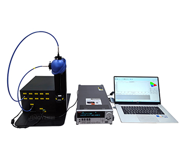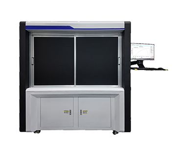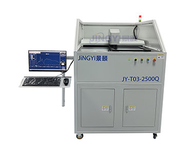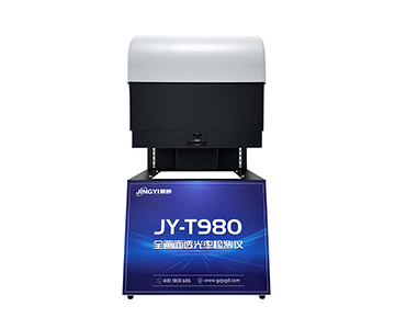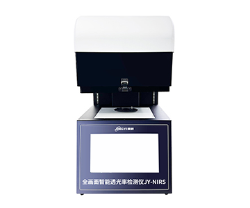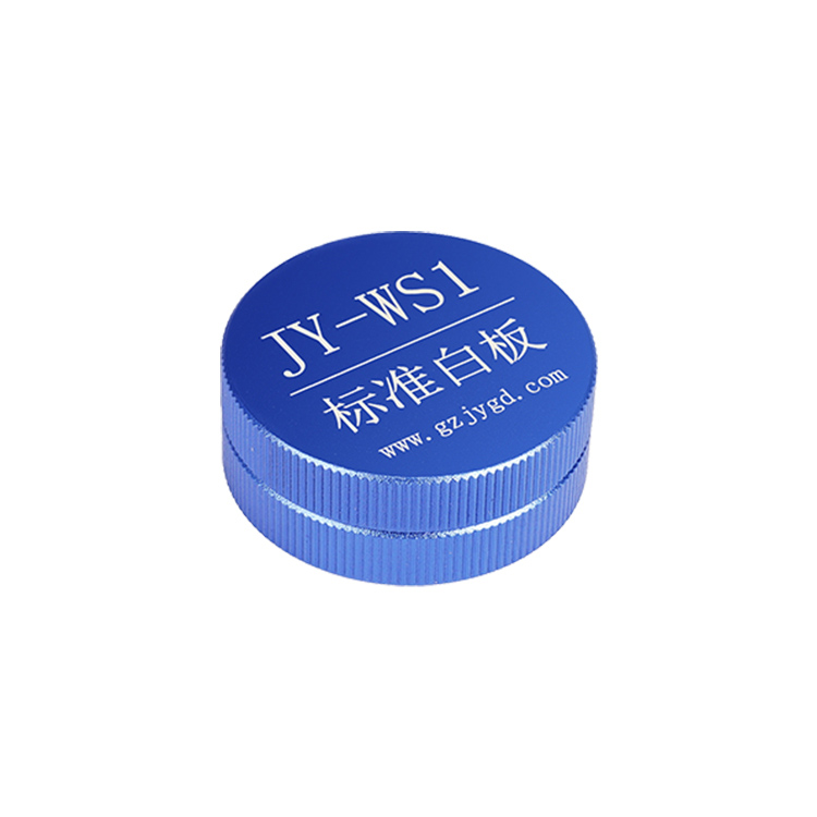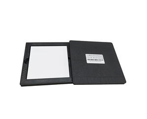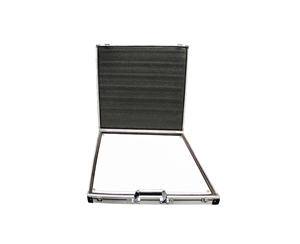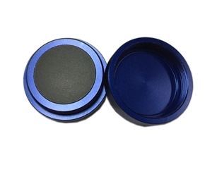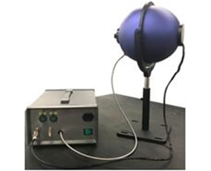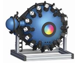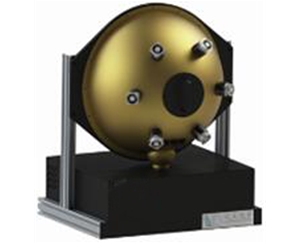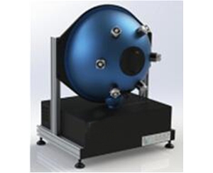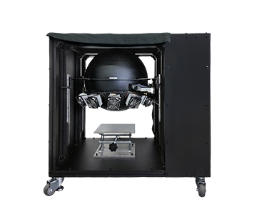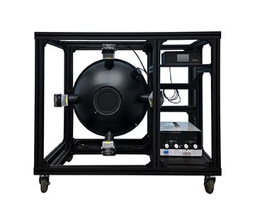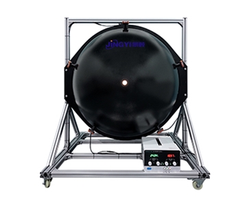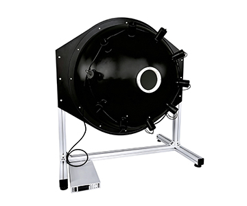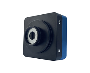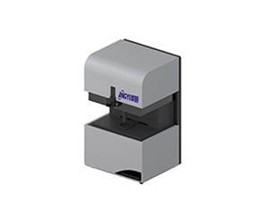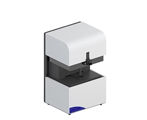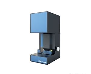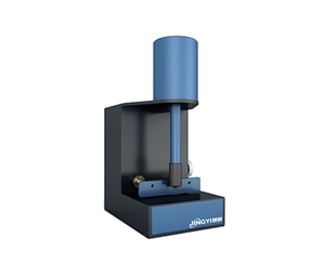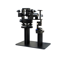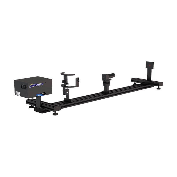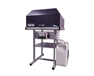
Mapping Measurement and Mapping Series
Optical Reflective Film Thickness Meter · Wafer-level Full-Wafer Mapping
Wafer-level mapping for circular surveying, 380-1100nm spectral interferometry, 15nm to 70μm non-contact thickness measurement, fully compatible with 2 to 12 inches
Product Introduction
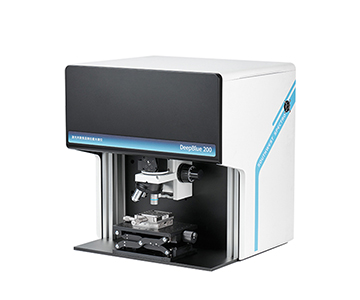
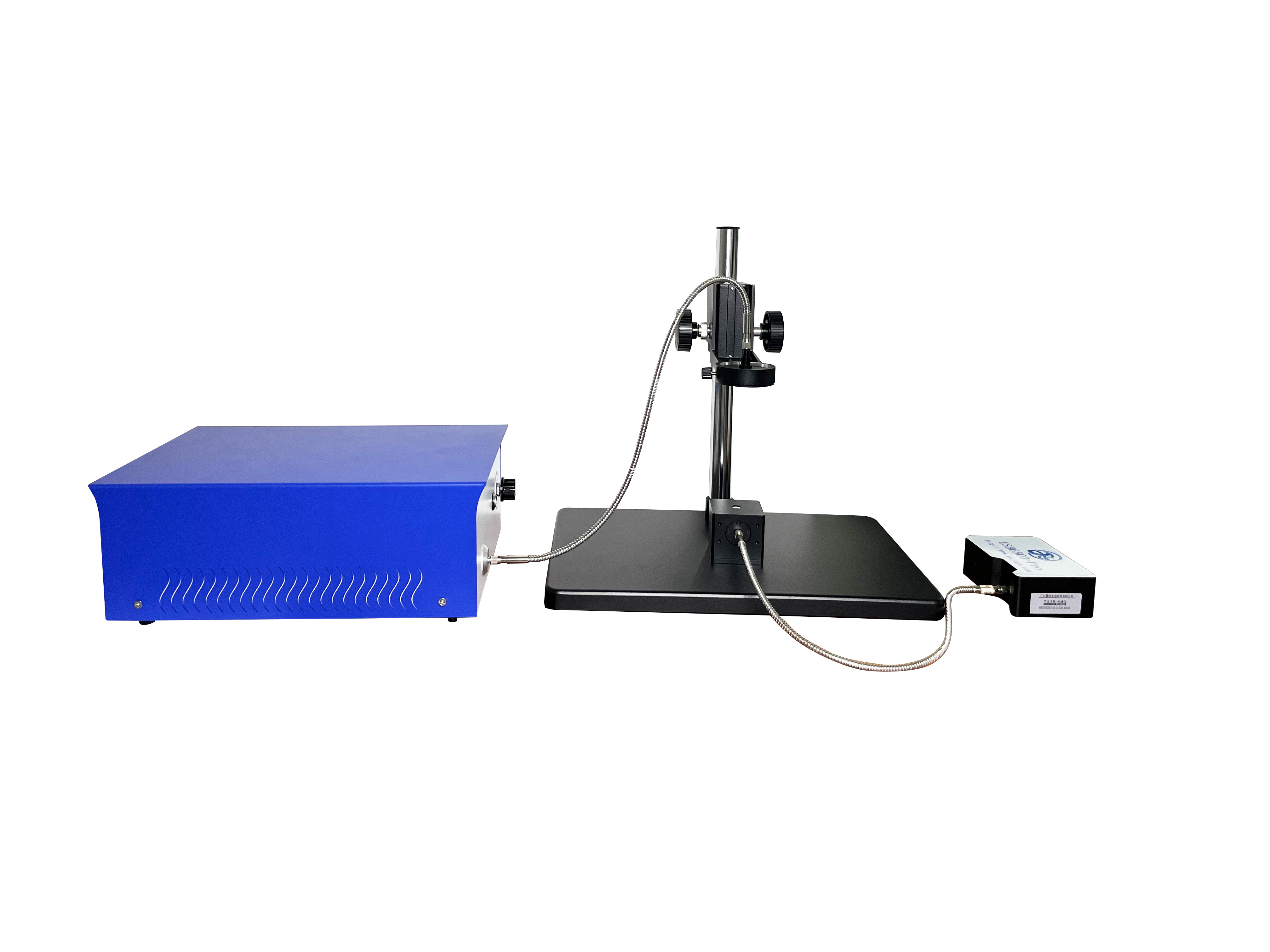
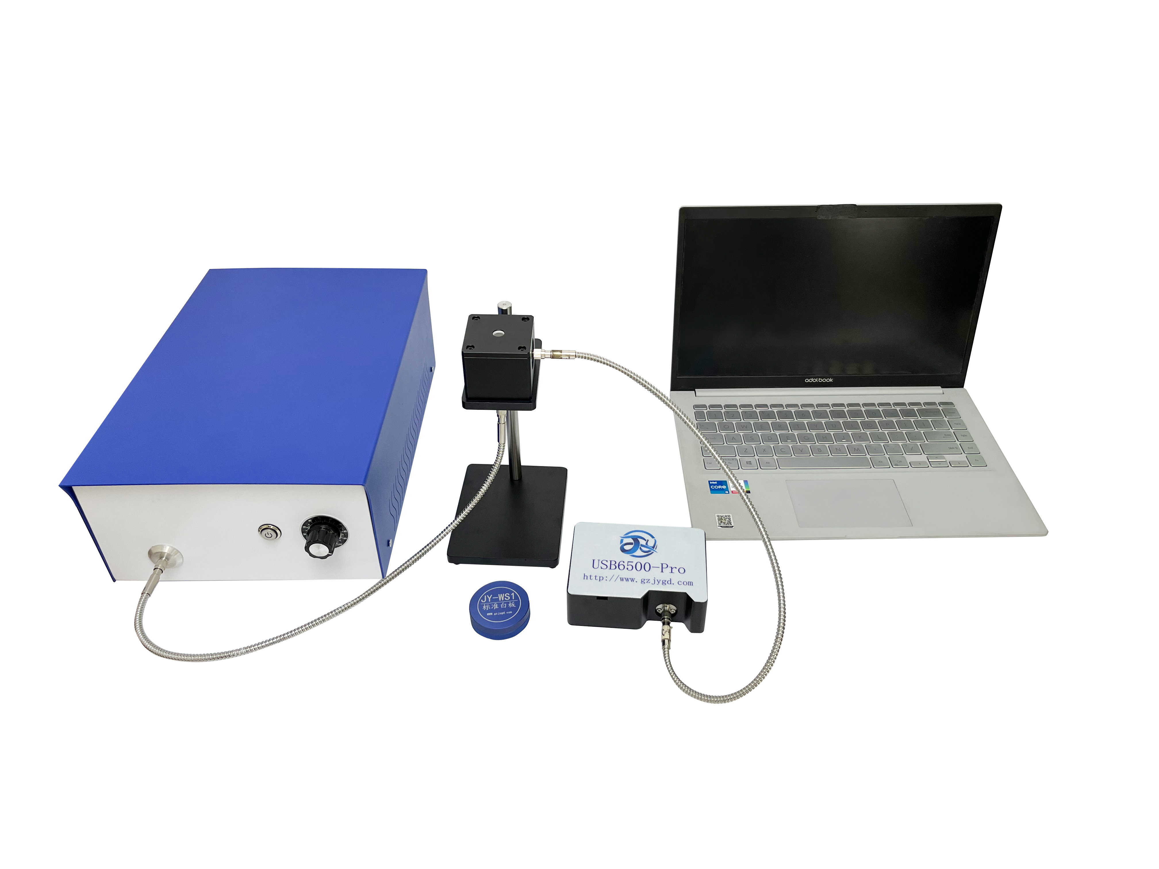
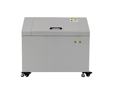
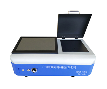
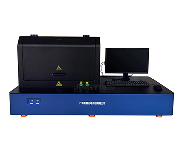
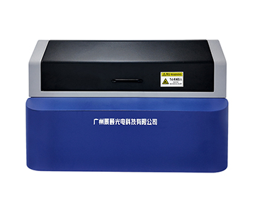
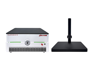
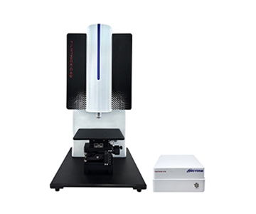
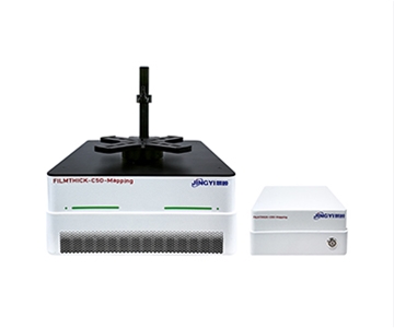
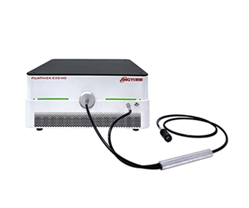
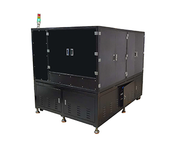
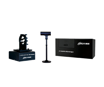
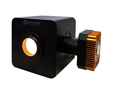
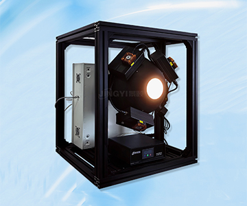
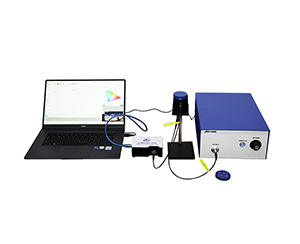
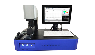
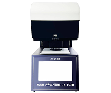
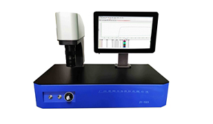
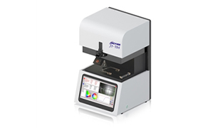
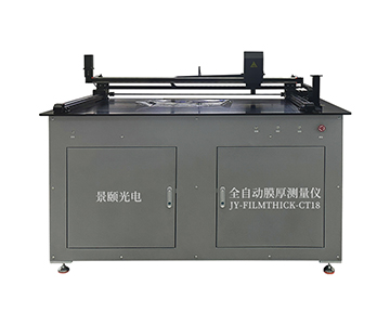
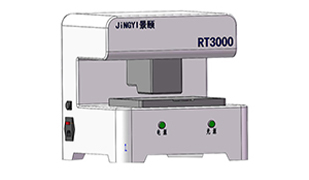
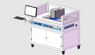
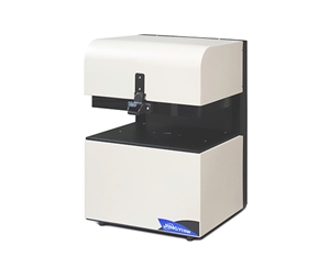
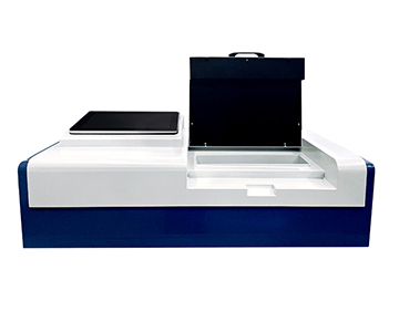
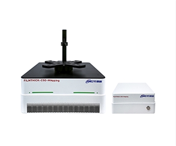
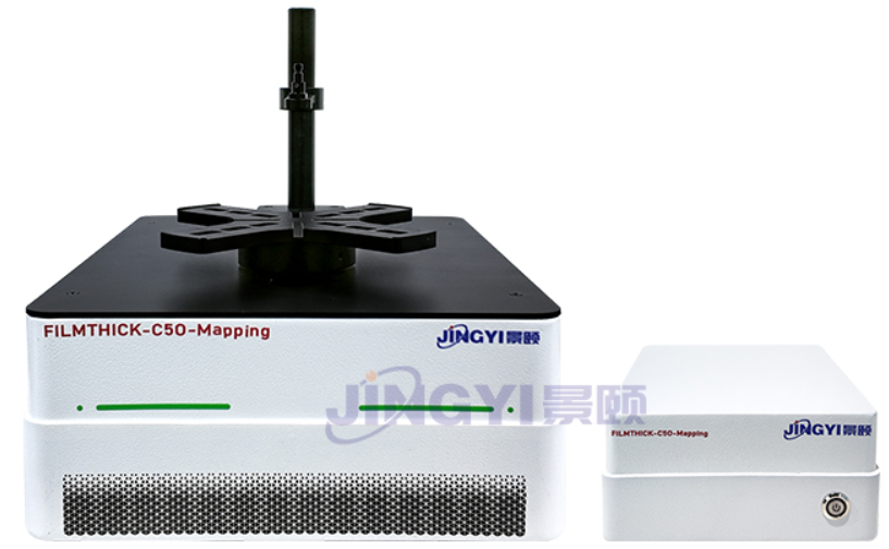
The FILMTHICK-C50-Mapping is a wafer-level Mapping measurement device designed for the semiconductor wafer, flat panel display, and precision optical coating industries. Based on the FILMTHICK-C series interferometric film thickness measurement platform, it integrates the R-Theta polar coordinate automatic movement platform, vacuum adsorption wafer stage, and dedicated Mapping measurement and mapping software. The device adopts the principle of reflective spectral interferometric thickness measurement, with a mechanical structure integrating imported long-life halogen tungsten lamp light sources. Combined with a self-developed high-precision spectrometer and three major inversion algorithms—FFT Fourier method, extreme value method, and fitting method—it achieves non-contact, non-destructive, high-precision measurement of wafers from 2 to 12 inches. It covers parameters such as single-layer and multilayer film thickness, refractive index n, extinction coefficient k, reflectivity, and color, and outputs full-sample two-dimensional and three-dimensional film thickness distribution maps.
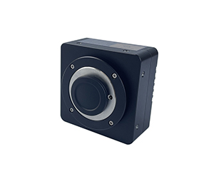
The OPTICAFILMTEST optical film thickness measurement software features a rich and open material refractive index database, which can display interference, FFT spectra, and film thickness trends in real time during measurement, assisting users in testing and analysis. The hardware adopts a modular design, with core components that can be independently replaced, facilitating subsequent functional expansion.
Core selling points
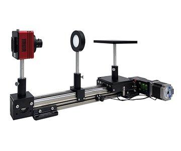
Wafer-level full-chip mapping: R-Theta polar coordinate automatic platform carries samples for radial and rotational degrees of freedom movement, with the optical system stationary and no assembly consistency differences between points; Automatically generates 2D contour cloud maps, 3D three-dimensional distribution maps, and profile lines;
Fast: single-point measurement time less than 0.5 seconds; 5 points / 5 seconds, 25 points / 14 seconds, 57 points / 30 seconds, significantly reducing detection cycles;
Wide range and high precision: single unit covers 15nm to 70μm, repeatability 0.2nm, stability better than 0.05nm, reducing equipment input and sample switching time;
Full specifications from 2 to 12 inches: 2 / 4 / 6 / 8 / 12 inch wafers can be placed directly on the chip, no need to purchase separate chucks by size;
Six types of scanning paths: circles and concentric circles / rectangles and squares / radial / center or edge removal / 4 fixed points / user-defined, also supports point programming and D distribution;
Measurement and simulation integrated: In addition to thickness inversion, it simultaneously provides refractive index n, extinction coefficient k, reflectance, and color; The built-in reflectance simulation module can assist in the development of new film process layers.
Core Technical Parameters (Standard Configuration Indicators)
|
Product Model
|
FILMTHICK-C50-Mapping
|
|
Optical Principle
|
Reflective Spectral Interferometry (White Light Interference), Non-contact, Non-destructive Measurement
|
|
Spectral Range
|
380nm - 1100nm (Visible to Near-Infrared)
|
|
Light Source
|
Mechanically integrated imported long-life halogen tungsten lamp light source, lifespan over 3000 hours
|
|
Measurement Spot Size
|
1.5mm (Standard configuration, optional according to sample requirements)
|
|
Film Thickness Measurement Range
|
15nm - 70μm
|
|
Film Thickness Repeatability Accuracy
|
0.2nm (Maximum value from 100 measurements on 100nm SiO₂/Si standard sample)
|
|
Film Thickness Absolute Accuracy
|
0.2% or 2nm (whichever is larger)
|
|
Film Thickness Stability
|
Better than 0.05nm
|
|
Measurable Parameters
|
Film thickness d, reflectance spectrum R(λ), color, refractive index n, extinction coefficient k
|
|
Reflectance Simulation
|
Supports modeling of different film layer structures and simulation of coating system reflectance curves
|
|
Algorithm Model
|
FFT Fourier method, extremum method, curve fitting method, supporting multi-layer film layer-by-layer fitting
|
|
Single Point Measurement Time
|
Less than 0.5 seconds
|
|
Mapping Scan Speed
|
5 points / 5 seconds; 25 points / 14 seconds; 57 points / 30 seconds
|
|
Sample Stage Type
|
R-Theta polar coordinate automatic moving stage (radial and rotational dual degrees of freedom)
|
|
Travel Range
|
Not less than 200mm × 200mm, extendable to 300mm × 300mm
|
|
Supported Sample Size
|
2-inch / 4-inch / 6-inch / 8-inch / 12-inch wafers
|
|
Manual Operation Movement Repeatability
|
±0.2mm (Maximum value from 100 measurements on 100nm SiO₂/Si sample)
|
|
Supported Scanning Paths
|
Circular / rectangular / square / radial / central or edge removal / 4-point / user-defined
|
|
Software
|
OPTICAFILMTEST Optical Film Thickness Measurement Software (Mapping Wafer Measurement Version), Windows 10 / 11 64-bit; built-in open refractive index material database
|
|
User Permissions
|
Manager / Operator / Controller three-level permission management
|
|
Data Export
|
CSV / Excel / XML and 2D, 3D graphical files
|
|
System Integration
|
Supports interfacing with upper-level MES / SPC systems (interfaces open according to projects)
|
|
Operating Environment
|
Temperature 18-28°C, humidity <80% without condensation; AC 220V±10%, 50Hz
|
|
Model
|
UV
|
UVX
|
Basic model
|
NIRX
|
NIR
|
|
Wavelength Range
|
190-1100nm
|
190-1700nm
|
380-1100nm
|
380-1700nm
|
950-1700nm
|
|
Light Source
|
Deuterium lamp, Halogen tungsten lamp
|
Halogen tungsten lamp
|
|
Thickness Range
|
1nm-40um
|
1nm-250um
|
10nm-100um
|
10um-250um
|
100um-250um
|
|
Accuracy
|
0.02nm
|
0.02nm
|
0.02nm
|
0.02nm
|
0.1nm
|
*The final right of interpretation of this technical specification belongs to the manufacturer.
Applicable Industries and Application Scenarios
Semiconductor Wafer Coating Uniformity
Flat Panel Display (FPD)
Precision Optical Coating
New Energy and Photovoltaics
Life Sciences and Biomedical
Micro-LED and Optical Communication
Typical Measured Film Data
|
Samples and Coatings
|
Measured Thickness
|
Application Areas
|
|
SiO₂ (Silicon Dioxide)
|
2108nm
|
Optical Coatings and Passivation Layers
|
|
ITO (Indium Tin Oxide)
|
36nm
|
Touch Screens and Smart Windows
|
|
Parylene
|
2490nm
|
Protective Layers for Medical Implants
|
|
Microlens Coating
|
3012nm
|
Optical Components
|
*The above accuracy indicators were measured on standard 100nm SiO₂/Si samples under room temperature conditions of 23±2℃. The actual measurement data comes from records of the FILMTHICK-C series on real customer samples, and the feasibility of measurements on specific samples is subject to the results of sample submission and actual measurement.
Branch Models (Same platform, branched according to sample type)
Branch models of FILMTHICK-C50-XY C50-Mapping
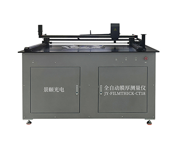
Designed for square and non-standard substrate samples. It uses an XY rectangular coordinate positioning displacement platform, allowing point collection and index editing or import in Cartesian coordinates, to acquire spectra point by point and invert the thickness. It is suitable for scenarios focusing only on a few designated inspection locations, as well as point measurements of rectangular, strip-shaped, or irregular substrates.
|
Wavelength Range
|
380nm - 1700nm (VIS and NIR dual detectors, seamless data stitching)
|
|
Film Thickness Measurement Range
|
10μm - 250μm (conventional coatings, medium to thick films preferred)
|
|
Film Thickness Repeatability
|
≤0.02nm
|
|
Film Thickness Absolute Accuracy
|
≤0.2% or 2nm (whichever is greater)
|
|
Platform Type
|
XY right-angle coordinate dual-axis precision motion platform (servo, ball screw, grating ruler closed-loop)
|
|
Effective Travel
|
300mm × 300mm, expandable to 400mm × 400mm
|
|
Positioning Accuracy
|
≤ ±5μm
|
|
Repeat Positioning Accuracy
|
≤ ±2μm
|
|
Minimum Step Size
|
1μm
|
|
Movement Speed
|
0 - 200mm/s
|
|
Point Capacity
|
Single recipe supports over 200 points
|
|
Point Arrangement
|
Matrix automatic generation / manual coordinate input / mouse click selection / CSV and Excel point table import
|
|
Overall Machine Configuration
|
Floor-standing integrated steel cabinet, approximately 600mm × 750mm × 1500mm
|
|
Safety Configuration
|
Front door observation window, door safety interlock, emergency stop button, compliant with IEC 60825-1
|
*The final right of interpretation of this technical specification belongs to the manufacturer.
Standard Configuration
|
Host (including self-developed high-precision spectrometer and optical path)
|
1 unit
|
|
Imported long-life halogen-tungsten lamp light source
|
1 set
|
|
Measurement software (pre-installed license, three-level permission management)
|
1 set
|
|
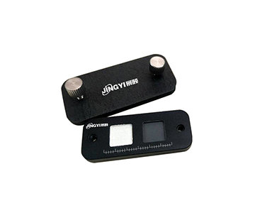
SiO₂/Si standard calibration samples
|
1 set
|
|
Chinese operation manual, software manual, and calibration certificate
|
1 set
|
|
Common tool kit and spare consumables
|
1 set
|
|
Remote diagnosis and online upgrade module
|
1 set
|
|
Transport packaging box
|
1 set
|
Service Commitment
|
Installation and Training
|
Provide online remote training and on-site installation services; after installation, operation training is conducted, covering instrument operation, software usage, measurement methods, and data analysis.
|
|
Warranty Period
|
One-year free warranty from the date of purchase; quality issues within the warranty period are repaired free of charge and faulty components are replaced; lifetime maintenance at cost price is provided after the warranty period.
|
|
Response Time
|
Response within 8 working hours on weekdays; first response within 4 hours in emergencies.
|
|
On-site Service Time
|
On-site service within 24 hours in Guangzhou and surrounding areas, within 48 hours in South China, and within 72 hours in major provincial capitals nationwide.
|
|
Spare Parts Support
|
Provide solutions for faulty components within 7 working days; commonly used consumables and vulnerable parts are stocked locally.
|
|
Calibration and Measurement
|
Provide national metrology institute or third-party traceable calibration certificates (CNAS optional).
|
|
Sample Testing
|
Before contract signing, free sample testing can be arranged, with actual measurement evaluation coefficients and repeatability data provided.
|
|
Software Upgrade
|
Free upgrades within the instrument’s service life (same model); remote diagnostics and online upgrade modules are provided.
|
Why Choose Jingyi Optoelectronics?
Independent R&D
The film thickness inversion algorithms (FFT Fourier method, extremum method, curve fitting method) and the OPTICAFILMTEST measurement software are all independently developed by our company; the spectral acquisition module uses a self-developed high-precision spectrometer.
National High-Tech Enterprise
Founded in 2013, our company is recognized as a National High-Tech Enterprise, a specialized and innovative enterprise, and a 'Little Giant' enterprise in technological innovation; we maintain long-term collaborations with universities and research institutes such as Tsinghua University and Peking University.
Localized Service
Our Guangzhou headquarters provides direct service nationwide, offering online remote training, on-site installation, remote fault diagnosis, and rapid spare parts delivery; the service chain is shorter compared to the indirect models of imported brands through agents.
Sample Testing Verification
Before signing a contract, we can arrange free sample testing, providing actual measurement evaluation coefficients and repeatability data as a basis for configuration confirmation and acceptance.
Consult customer service to obtain detailed materials and exclusive solutions.
Tel: 400-1800-685
Email:info@gzjygd.com