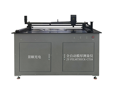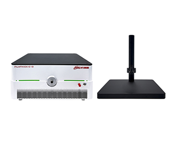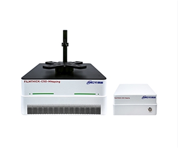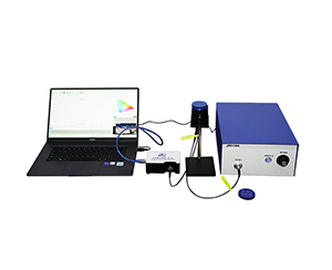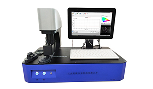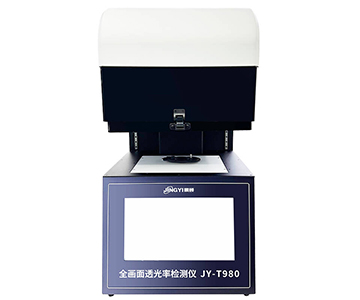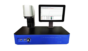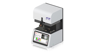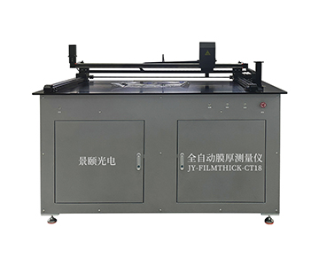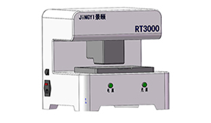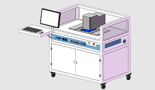
Microscopic Series
Microscopic Film Thickness Meter · Micro-area and Patterned Samples
Microscopic Imaging System · Submicron Positioning · Observable Micron-scale Thin Film Structures · Micro-area and Patterned Samples
Product Introduction
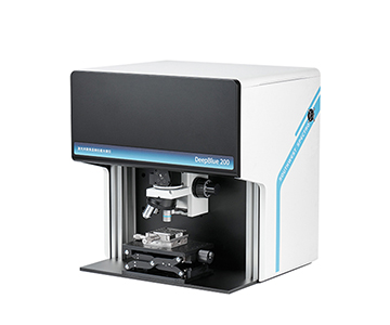
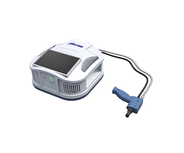
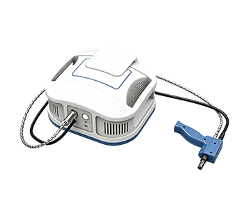
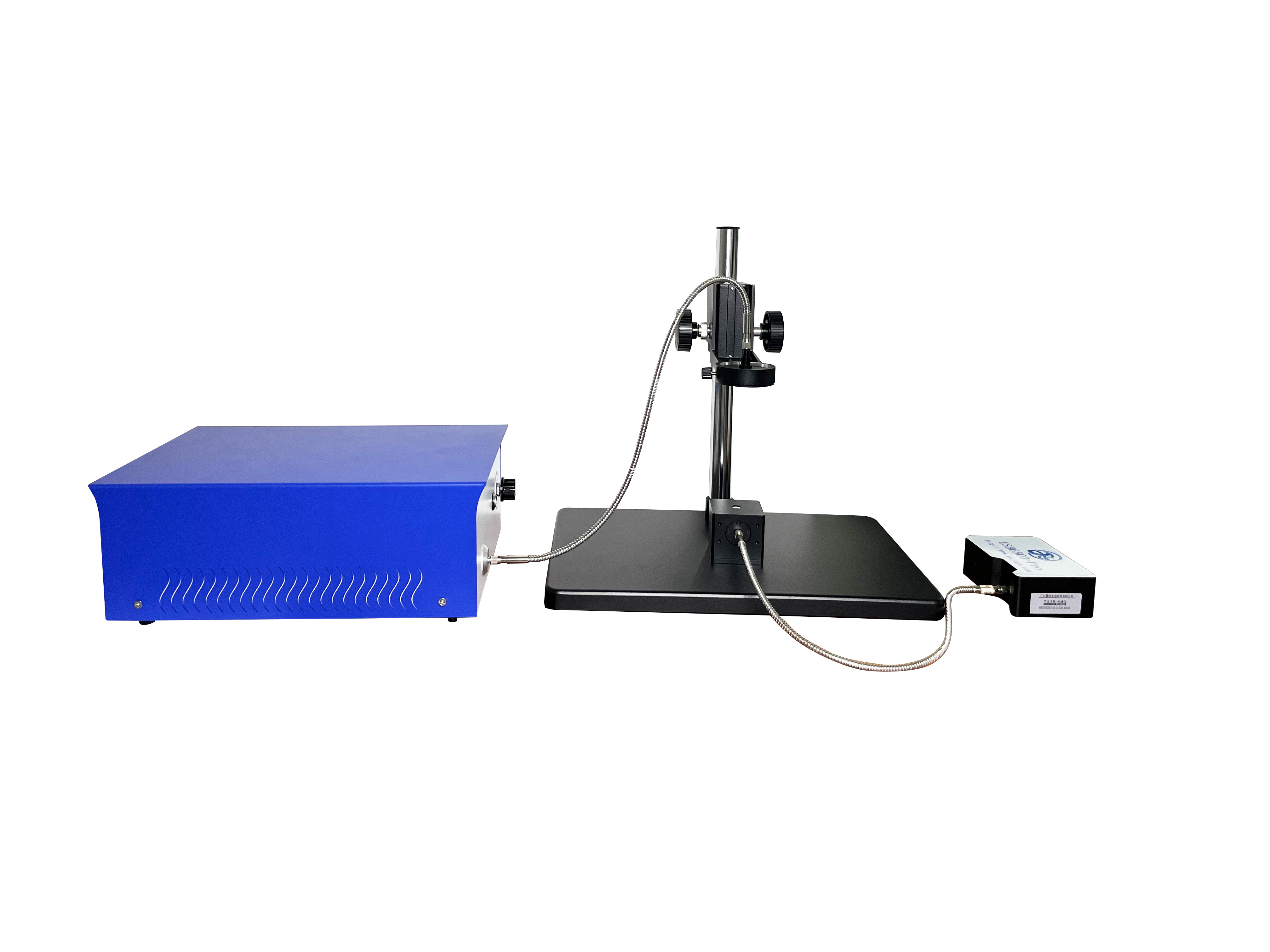
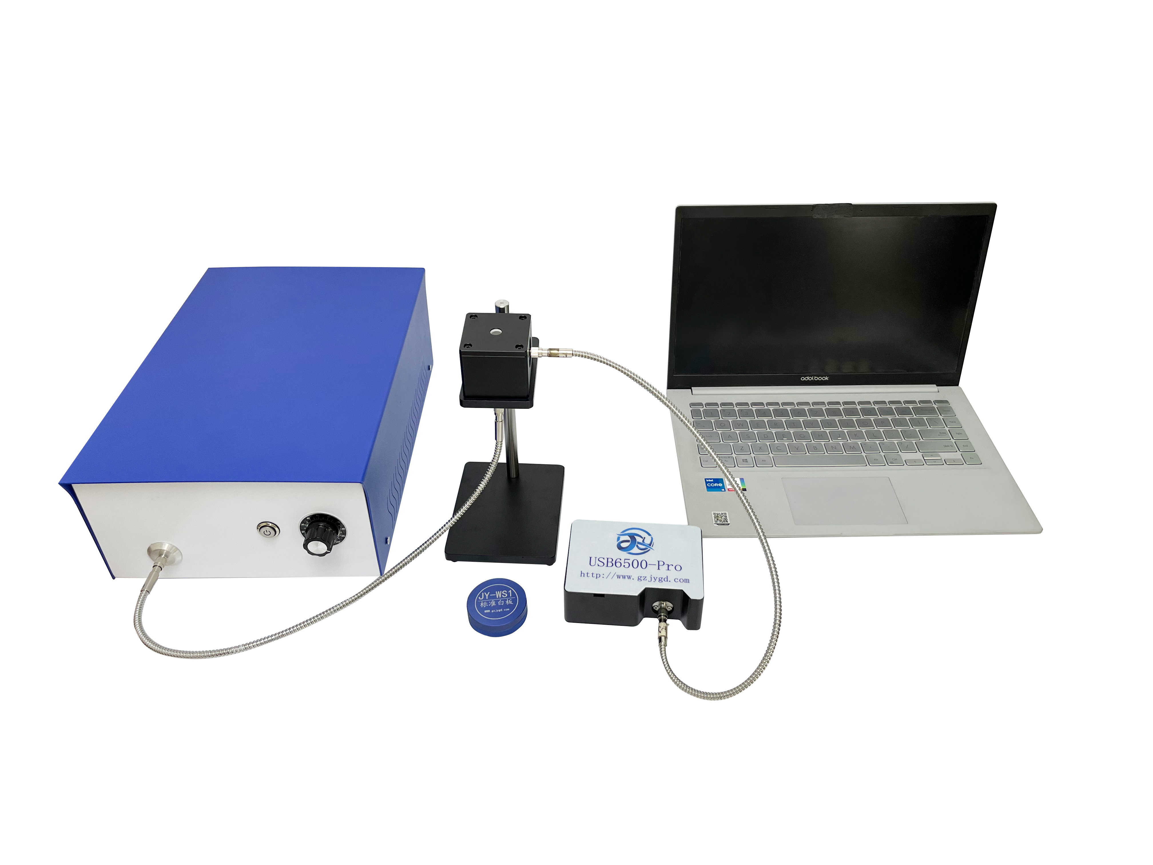
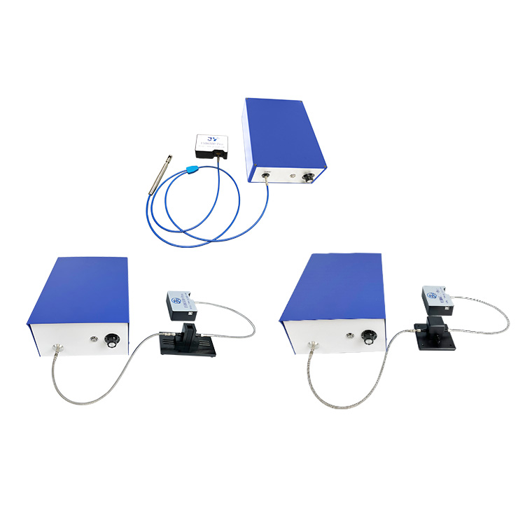
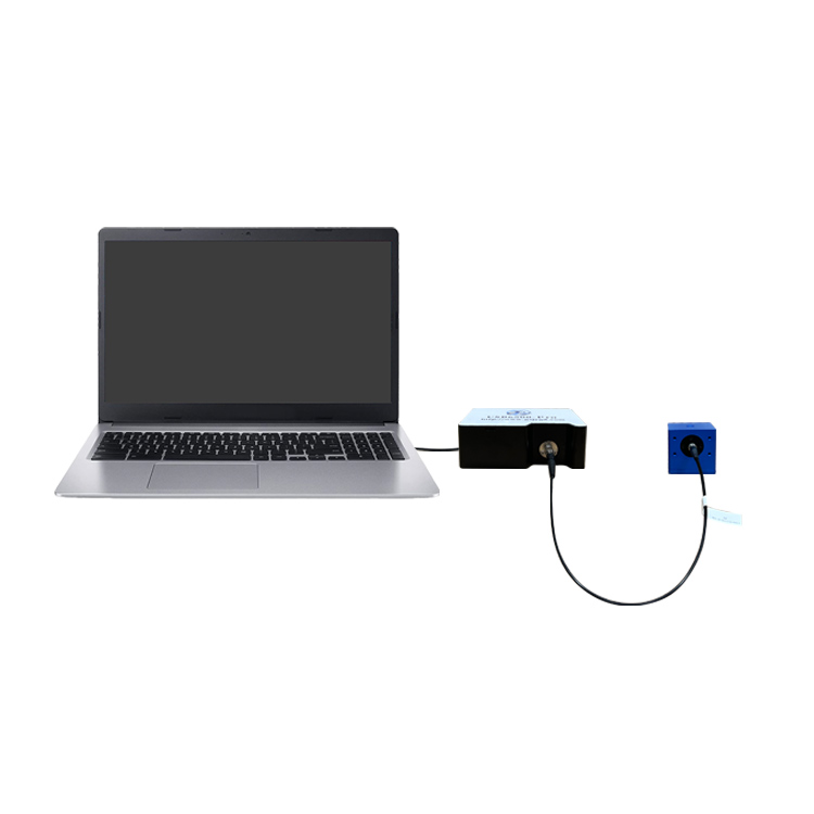
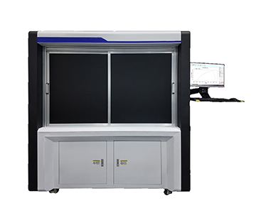
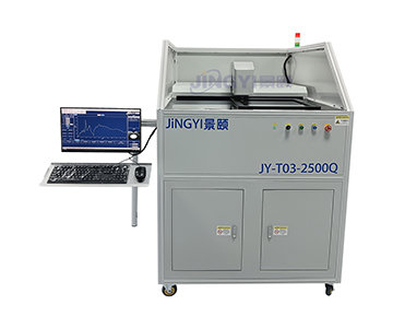
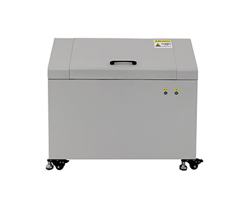
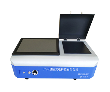
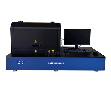
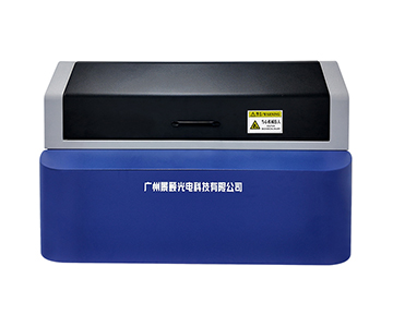
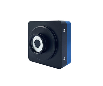
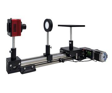
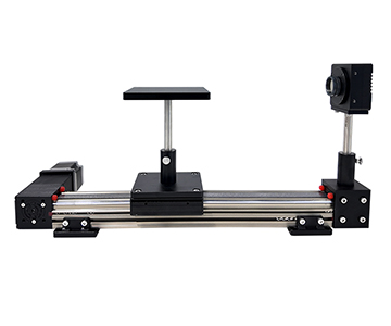
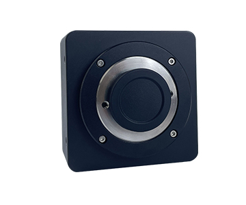
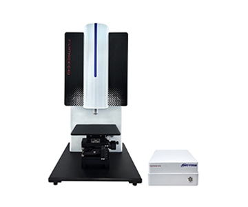
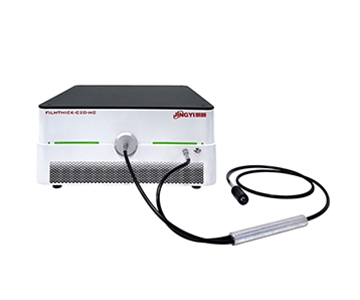
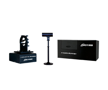
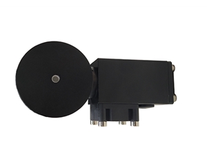
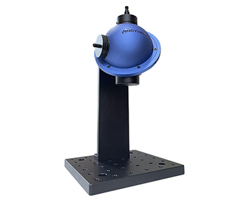
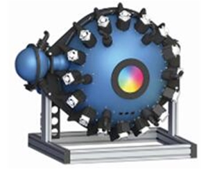
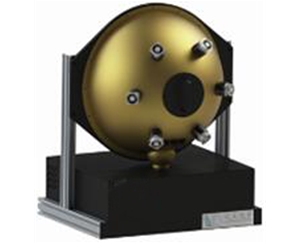
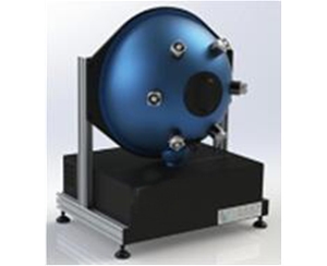
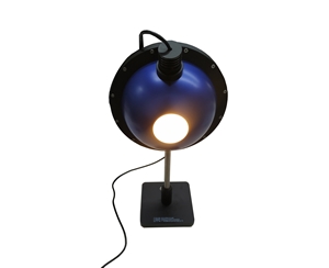
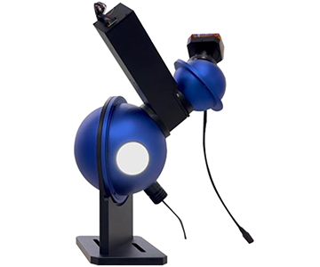
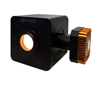
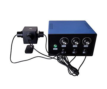
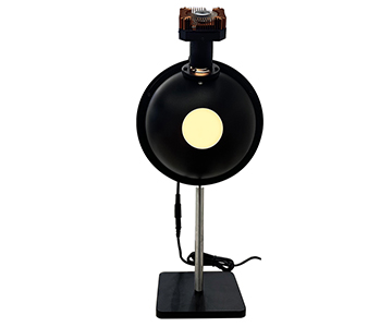
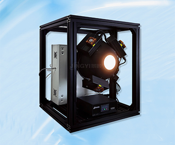
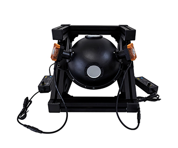
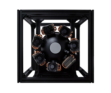
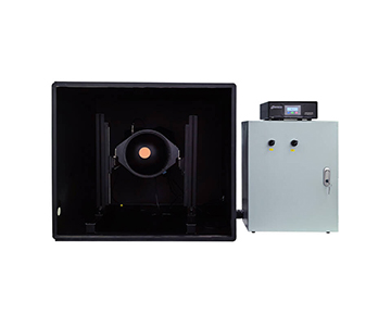
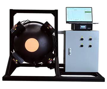
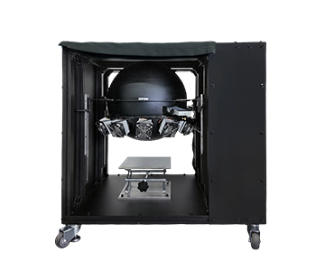
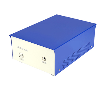
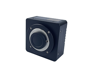
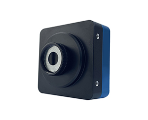
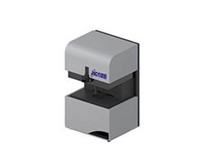
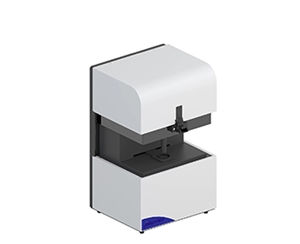
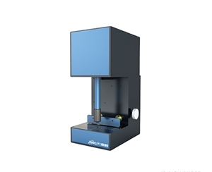
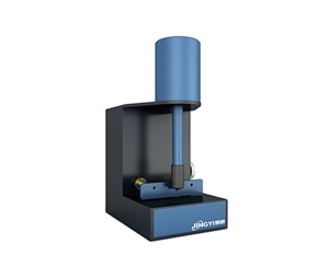
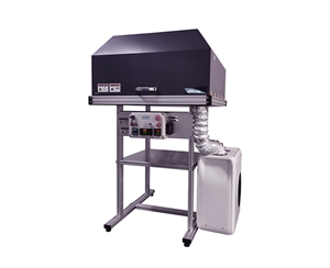
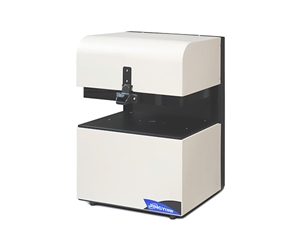
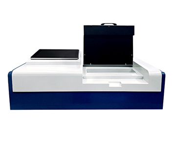
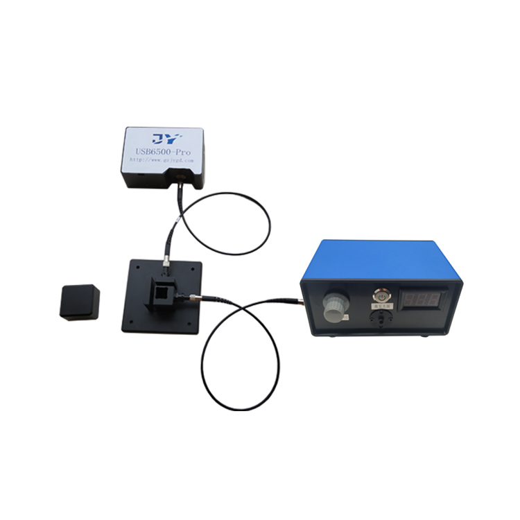
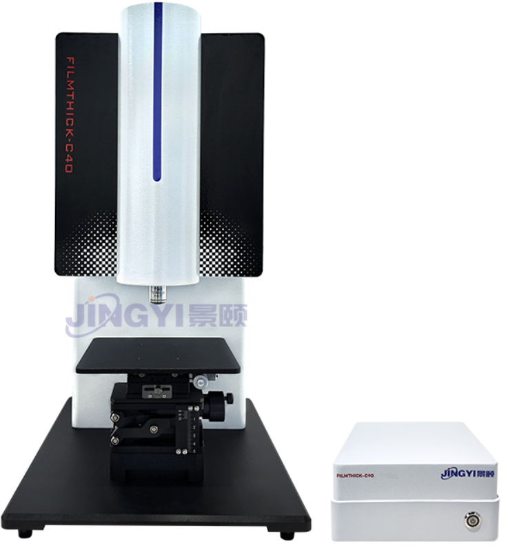
The FILMTHICK-C40 Microscopic Series is designed for film thickness measurement on patterned wafers, micro-area devices, optical components, and other small-area and patterned samples. The equipment adopts a reflective spectral interferometry measurement principle, with a mechanical structure integrating imported long-life halogen tungsten light sources, cooperating with a self-developed high-precision spectrometer and three inversion algorithms (FFT Fourier method, extrema method, and fitting method) to achieve non-contact, non-destructive, high-precision measurements on samples. It covers single-layer and multi-layer film thickness, refractive index n, extinction coefficient k, reflectivity, and color parameters. Using a vertical microscopic optical path structure and microscopic imaging system, micron-scale thin film structures can be directly observed, combining the observation of the measurement area and film thickness inversion within the same optical path. The blue scale positioning precision can reach the submicron level.
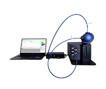
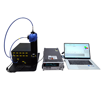
The accompanying OPTICAFILMTEST optical film thickness measurement software has a rich, open material refractive index database built in. During measurement, interference patterns, FFT spectra, and film thickness trends can be displayed in real time to assist users in test analysis. The hardware uses a modular design, allowing core components to be independently replaced for future functional expansion and supports shared wavelength range selections with the C10 platform.
Key Selling Points
Microscopic Imaging System: Directly observes micron-scale film structures; the measurement area is visualized, facilitating alignment, interpretation, and result verification;
Submicron-level Positioning: Blue scale positioning precision reaches submicron level, suitable for accurate positioning on patterned samples and micro-area devices;
Vertical Structure Design: Vertical microscopic optical path and support structure facilitate alignment, observation, and repeatable positioning of micro-area samples;
Micro-area and Patterned Samples: Designed for measuring film thickness on patterned wafers, micro-area devices, optical components, and other small-area samples, overcoming the limitation of large spot sizes in conventional benchtop models;
Selectable Wavelength Bands: Shares wavelength range system with the C10 platform, with options such as 190-1100nm / 190-1700nm / 380-1100nm / 380-1700nm;
Same Source as C10 Platform: Shares FFT / extrema / fitting algorithms and the OPTICAFILMTEST measurement software with the C10 platform, including a built-in open material refractive index database, with interoperable formulations and data formats.
Core Technical Parameters (Standard Configuration Indicators)
|
Optical Principles
|
Reflective spectroscopic interferometry, non-contact, non-destructive measurement
|
|
Structural Forms
|
Vertical microscope optical path structure, including microscopic imaging system
|
|
Positioning Methods
|
Blue scale positioning, positioning accuracy can reach sub-micron level
|
|
Sample Adaptation
|
Graphical wafer, micro-device, optical component and other small regions and patterned samples
|
|
Spectral Configuration
|
Shares gear system with C10 platform, 380-1100nm (basic) and other wavelength ranges optional
|
|
Light Source
|
Imported long-life halogen-tungsten lamp integrated into mechanical structure, lifespan ≥10,000 hours
|
|
Algorithm Models
|
FFT Fourier method, extremum method, curve fitting method; supports layer-by-layer fitting of multi-layer films
|
|
Measurable Parameters
|
Film thickness d, reflectance spectrum R(λ), color, refractive index n, extinction coefficient k
|
|
Software
|
OPTICAFILMTEST optical film thickness measurement software, Windows 10 / 11 64-bit; built-in open material refractive index database, supports CSV / Excel / XML / PDF report export
|
|
Working Environment
|
Temperature 18-28°C, humidity <80% without condensation; AC 220V±10%, 50Hz
|
|
Model
|
UV
|
UVX
|
Basic model
|
NIRX
|
NIR
|
|
Wavelength Range
|
190-1100nm
|
190-1700nm
|
380-1100nm
|
380-1700nm
|
950-1700nm
|
|
Light Source
|
Deuterium lamp, Halogen tungsten lamp
|
Halogen tungsten lamp
|
|
Thickness Range
|
1nm-40um
|
1nm-250um
|
10nm-100um
|
10um-250um
|
100um-250um
|
|
Accuracy
|
0.02nm
|
0.02nm
|
0.02nm
|
0.02nm
|
0.1nm
|
*The final right of interpretation of this technical specification belongs to the manufacturer.
Key Points of Microscale Measurement (Measurement Capability for Small Areas and Patterned Samples)
|
Microzone Positioning
|
The blue scale positioning accuracy can reach sub-micron levels, working with the microscopic imaging system to precisely target tiny areas.
|
|
Observation and Measurement on the Same Optical Path
|
The microscopic imaging system can directly observe micrometer-thin film structures, with a visualized measurement area that makes alignment and result verification easier.
|
|
Wavelength Selection
|
It shares the wavelength band system with the C10 platform, allowing selection of 380-1100nm bands based on film and substrate matching.
|
|
Sample Adaptation
|
Graphical visualization of small areas and patterned samples like wafers, micro-devices, and optical components.
|
Applicable Industries and Application Scenarios
Graphical Wafers and Microregion Devices
Optical Components and Filters
Perovskite and Quantum Dot Thin Films
Photoresist and Dielectric Films
Microregion Film Layers of Display Panels
University Research and New Material Characterization
Typical Measured Film Data
|
Samples and Film Layers
|
Measured Thickness
|
Application Fields
|
|
Perovskite
|
16.7nm
|
Perovskite Solar Cells
|
|
Quantum Dots (QD)
|
34.3nm
|
QLED Displays
|
|
Photoresist
|
72nm
|
Semiconductor Photolithography Processes
|
|
Microlens Coating
|
3012nm
|
Optical Components
|
*The detailed technical specifications and microscopic optical path specifications of this series are subject to the latest specification sheets. The measured data in the above table come from actual customer sample measurement records, and the feasibility of specific samples shall be based on actual test results of submitted samples.
Standard Configuration
|
Host (including self-developed high-precision spectrometer and optical path)
|
1 unit
|
|
Imported long-life halogen-tungsten lamp light source
|
1 set
|
|
Measurement software (pre-installed license, three-level permission management)
|
1 set
|
|
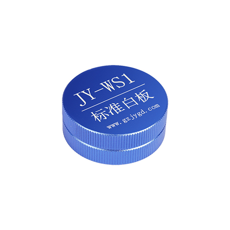
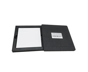
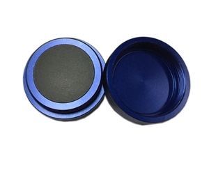
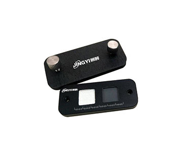
SiO₂/Si standard calibration samples
|
1 set
|
|
Chinese operation manual, software manual, and calibration certificate
|
1 set
|
|
Common tool kit and spare consumables
|
1 set
|
|
Remote diagnosis and online upgrade module
|
1 set
|
|
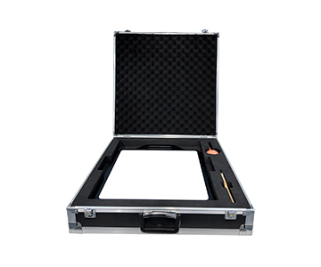
Transport packaging box
|
1 set
|
Service Commitment
|
Installation and Training
|
Provide online remote training and on-site installation services; after installation, operation training is conducted, covering instrument operation, software usage, measurement methods, and data analysis.
|
|
Warranty Period
|
One-year free warranty from the date of purchase; quality issues within the warranty period are repaired free of charge and faulty components are replaced; lifetime maintenance at cost price is provided after the warranty period.
|
|
Response Time
|
Response within 8 working hours on weekdays; first response within 4 hours in emergencies.
|
|
On-site Service Time
|
On-site service within 24 hours in Guangzhou and surrounding areas, within 48 hours in South China, and within 72 hours in major provincial capitals nationwide.
|
|
Spare Parts Support
|
Provide solutions for faulty components within 7 working days; commonly used consumables and vulnerable parts are stocked locally.
|
|
Calibration and Measurement
|
Provide national metrology institute or third-party traceable calibration certificates (CNAS optional).
|
|
Sample Testing
|
Before contract signing, free sample testing can be arranged, with actual measurement evaluation coefficients and repeatability data provided.
|
|
Software Upgrade
|
Free upgrades within the instrument’s service life (same model); remote diagnostics and online upgrade modules are provided.
|
Why Choose Jingyi Optoelectronics?
Independent R&D
The film thickness inversion algorithms (FFT Fourier method, extremum method, curve fitting method) and the OPTICAFILMTEST measurement software are all independently developed by our company; the spectral acquisition module uses a self-developed high-precision spectrometer.
National High-Tech Enterprise
Founded in 2013, our company is recognized as a National High-Tech Enterprise, a specialized and innovative enterprise, and a 'Little Giant' enterprise in technological innovation; we maintain long-term collaborations with universities and research institutes such as Tsinghua University and Peking University.
Localized Service
Our Guangzhou headquarters provides direct service nationwide, offering online remote training, on-site installation, remote fault diagnosis, and rapid spare parts delivery; the service chain is shorter compared to the indirect models of imported brands through agents.
Sample Testing Verification
Before signing a contract, we can arrange free sample testing, providing actual measurement evaluation coefficients and repeatability data as a basis for configuration confirmation and acceptance.
Consult customer service to obtain detailed materials and exclusive solutions.
Tel: 400-1800-685
Email:info@gzjygd.com